Semiconductor stacking layer and fabricating method thereof

a technology of semiconductor devices and stacking layers, which is applied in the direction of semiconductor devices, electrical equipment, basic electric elements, etc., can solve the problems of adversely affecting the characteristics of semiconductor devices, defects on the interface between c-si and other thin films, etc., and achieve the effect of reducing the defects between the a-si layer and the doped c-si layer

Active Publication Date: 2012-05-29
AU OPTRONICS CORP
View PDF2 Cites 0 Cited by
  • Summary
  • Abstract
  • Description
  • Claims
  • Application Information

AI Technical Summary

Benefits of technology

[0010]The present application is further directed to a fabricating method of a semiconductor stacking layer. By applying the method, interface defects existing between an a-Si layer and a doped μc-Si layer in the semiconductor stacking layer can be reduced in an effective manner.
[0019]Based on the above, the surface treatment is performed on the surface of the a-Si layer before the doped μc-Si layer is deposited onto the a-Si layer, such that the treated surface of the a-Si layer is conducive to subsequent growth of the doped μc-Si layer according to the present application. Thereby, the interface defects between the a-Si layer and the doped μc-Si layer can be effectively reduced.

Problems solved by technology

Nonetheless, when μc-Si is applied to fabrication of TFTs or other semiconductor devices, there exist defects on interfaces between μc-Si and other thin films because of the difference between the properties of μc-Si and those of the thin films.
These defects adversely affect characteristics of the semiconductor devices.

Method used


Image

  • Semiconductor stacking layer and fabricating method thereof
  • Semiconductor stacking layer and fabricating method thereof
  • Semiconductor stacking layer and fabricating method thereof

Examples


first embodiment

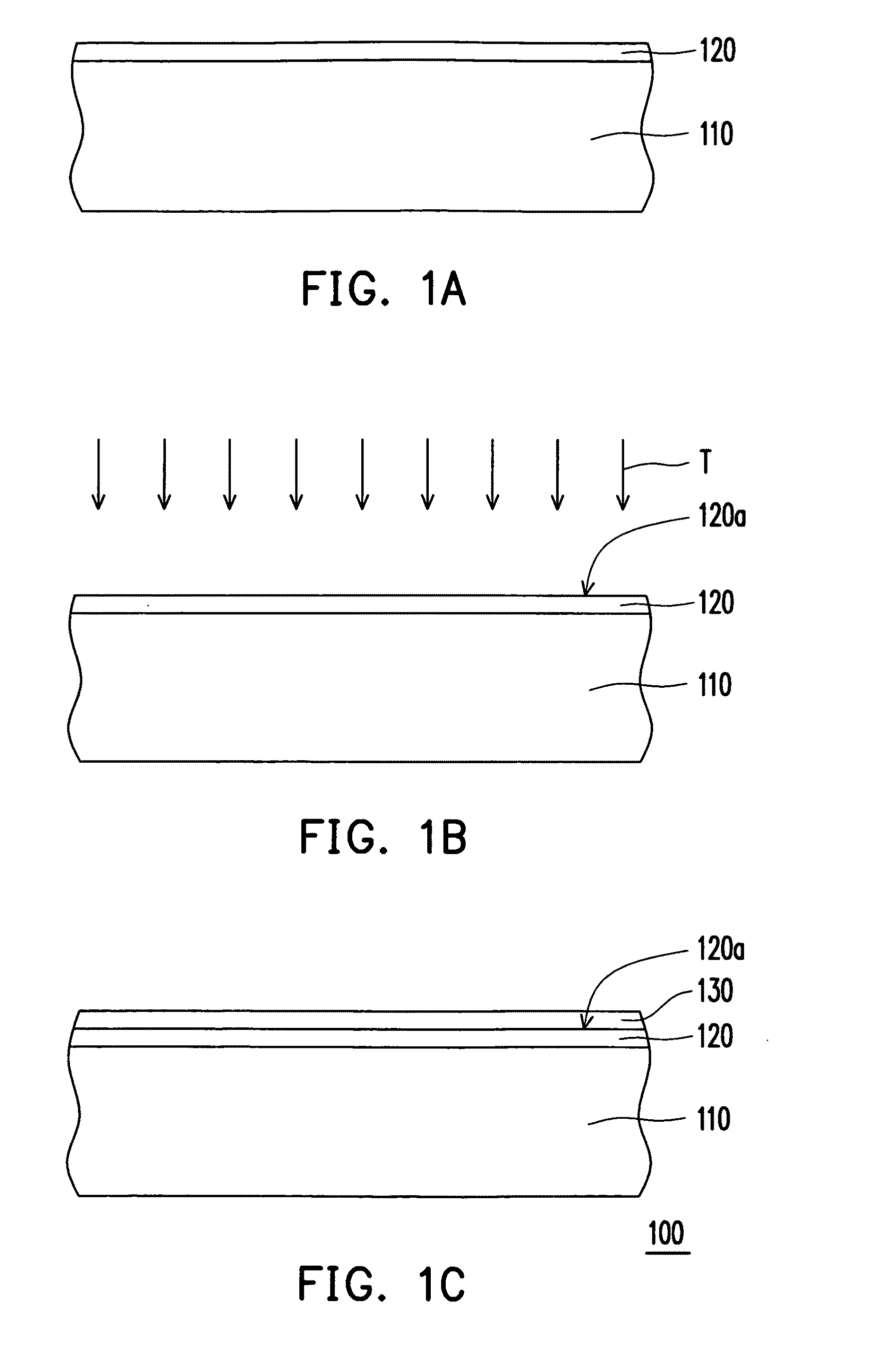
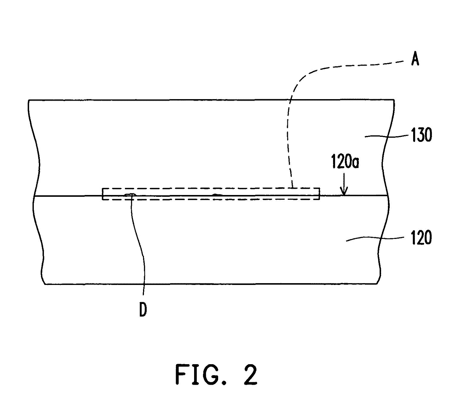
[0027]FIGS. 1A to 1C are schematic cross-sectional views illustrating a fabricating method of a semiconductor stacking layer according to an embodiment of the present invention. Referring to FIG. 1A, first, an a-Si layer 120 is formed on a substrate 110. Next, referring to FIG. 1B, after formation of the a-Si layer 120, surface treatment T is performed on a surface 120a of the a-Si layer 120. Thereby, silicon atoms on the surface 120a of the a-Si layer 120 can be orderly arranged. Namely, after the surface treatment T is performed, the treated surface 120a of the a-Si layer 120 is conducive to subsequent formation of a doped μc-Si layer 130.

[0028]In the present embodiment, the surface treatment T refers to pretreatment performed on the surface 120a of the a-Si layer 120 with use of hydrogen (H2) plasma. Specifically, the H2 plasma improves structural compactness of the surface 120a of the a-Si layer 120 so as to enhance bonding strength between the a-Si layer 120 and the doped μc-Si...

second embodiment

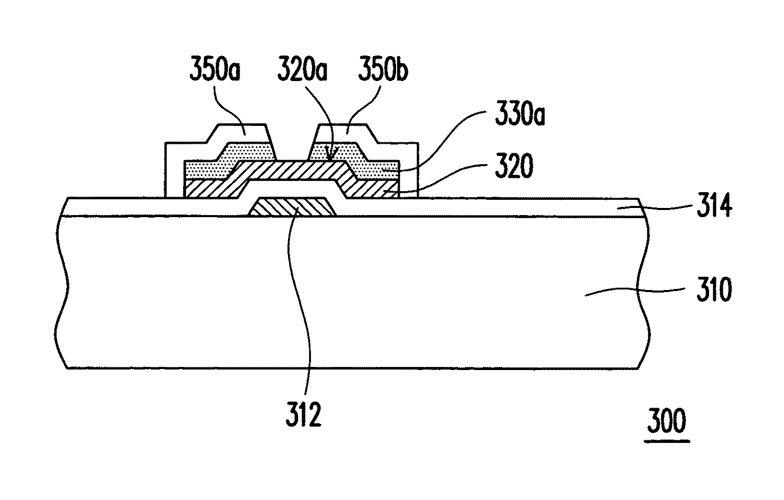
[0032]FIGS. 3A to 3D are schematic cross-sectional views illustrating a fabricating method of a TFT according to an embodiment of the present invention. Referring to FIG. 3A, in the present embodiment, a gate 312 and a gate insulation layer 314 are formed on the substrate 310. In particular, the gate 312 is formed by first forming a gate material layer (not shown) on the substrate 310. Next, the gate material layer is patterned to form the gate 312. Thereafter, the gate insulation layer 314 is formed on the gate 312 and the substrate 310. Finally, an a-Si layer 320 is formed on the gate insulation layer 314, as indicated in FIG. 3A.

[0033]Referring to FIG. 3B, after formation of the a-Si layer 320, surface treatment T is performed on a surface 320a of the a-Si layer 320. Thereby, silicon atoms on the surface 320a of the a-Si layer 320 can be orderly arranged. Namely, after the surface treatment T is performed, the treated surface 320a of the a-Si layer 320 is conducive to subsequent ...


PUM

PropertyMeasurementUnit
thicknessaaaaaaaaaa
widthaaaaaaaaaa
thicknessaaaaaaaaaa

Abstract

A fabricating method of a semiconductor stacking layer includes following steps. First, an amorphous silicon (a-Si) layer is formed on a substrate. Surface treatment is then performed on a surface of the a-Si layer. After that, a doped microcrystalline silicon (μc-Si) layer is formed on the treated surface of the a-Si layer, wherein interface defects existing between the a-Si layer and the doped μc-Si layer occupy an area in a cross-sectional region having a width of 1.5 micrometers and a thickness of 40 nanometers, and a ratio of the occupied area in the cross-sectional region is equal to or less than 10%. The method of fabricating the semiconductor stacking layer can be applied to a fabrication process of a semiconductor device to effectively reduce the interface defects of the semiconductor stacking layer.

Description

CROSS-REFERENCE TO RELATED APPLICATION[0001]This application claims the priority benefit of Taiwan application serial no. 98112349, filed on Apr. 14, 2009. The entirety of the above-mentioned patent application is hereby incorporated by reference herein and made a part of specification.BACKGROUND OF THE INVENTION[0002]1. Field of the Invention[0003]The present application relates to a semiconductor stacking layer and a fabricating method thereof. More particularly, the present application relates to a semiconductor stacking layer composed of an amorphous silicon (a-Si) layer and a microcrystalline silicon (μc-Si) layer and a fabricating method of the semiconductor stacking layer.[0004]2. Description of Related Art[0005]In recent years, due to the mature optoelectronic technology and the advanced semiconductor fabrication technology, flat panel displays are developed rapidly. Among the flat panel displays, thin film transistor liquid crystal displays (TFT-LCDs) having advantages of l...

Claims


Application Information

Patent Timeline
Patent Type & Authority Patents(United States)
IPC IPC(8): H01L29/04
CPCH01L21/0245H01L21/02513H01L21/02532H01L21/02595H01L21/02658H01L29/66765H01L29/78618
Inventor HOU, CHIH-YUAN
Owner AU OPTRONICS CORP
Why Eureka
Try Eureka