Semiconductor structure and fabrication method thereof

a technology of semiconductors and structures, applied in the direction of semiconductor devices, semiconductor/solid-state device details, electrical apparatus, etc., can solve the problems of poor performance of formed semiconductor structures, insufficient area of wafers for interconnection wires for conventional circuits,

Active Publication Date: 2019-01-31
SEMICON MFG INT (SHANGHAI) CORP +1
View PDF0 Cites 2 Cited by
  • Summary
  • Abstract
  • Description
  • Claims
  • Application Information

AI Technical Summary

Problems solved by technology

Correspondingly, a wafer may not provide enough area to form interconnecting wires for conventional circuits.
The formed semiconductor structures have poor performances.

Method used


Image

  • Semiconductor structure and fabrication method thereof
  • Semiconductor structure and fabrication method thereof
  • Semiconductor structure and fabrication method thereof

Examples


Embodiment Construction

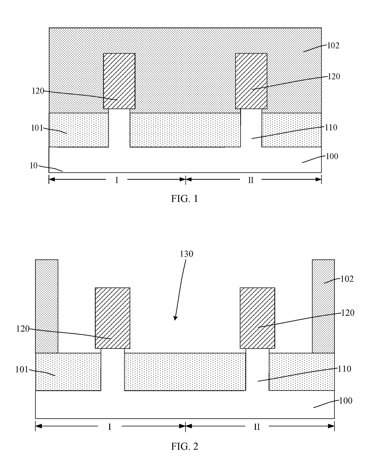
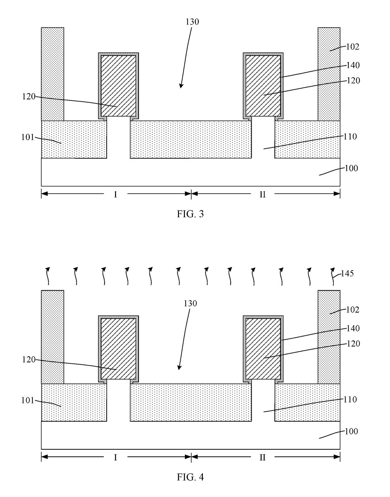
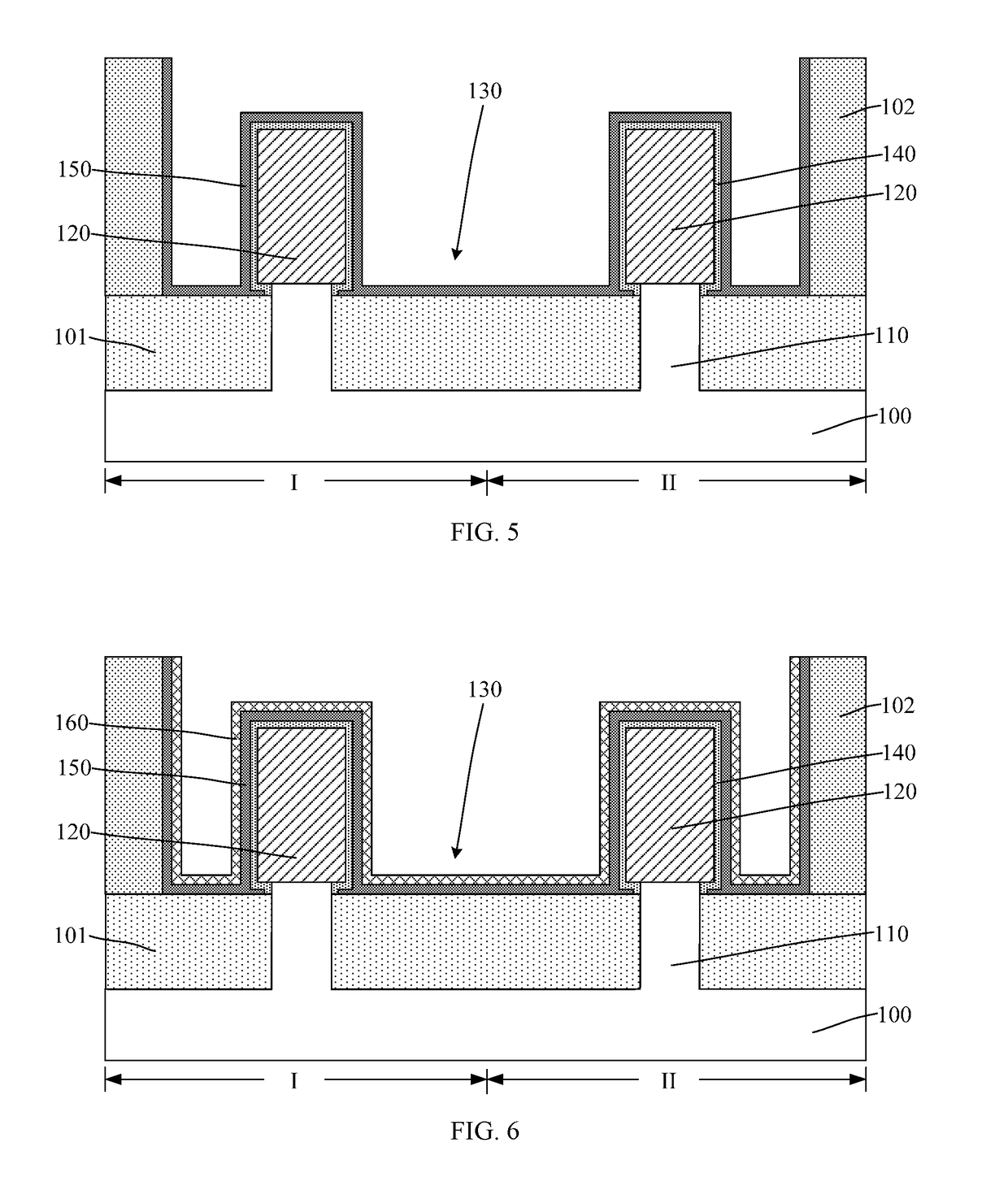
[0012]Reference will now be made in detail to exemplary embodiments of the disclosure, which are illustrated in the accompanying drawings. Wherever possible, the same reference numbers will be used throughout the drawings to refer to the same or like parts.

[0013]To reduce the contact resistances between the conductive plugs in the contact openings and the semiconductor devices, metal silicide layers are formed to form low-ohm contacts between the conductive plugs in the contact openings and doped epitaxial layers.

[0014]The metal silicide layers are formed by reacting metal layers with doped epitaxial layers. As process nodes of the integrated circuits and the critical dimensions of the devices continuously decrease, spaces for forming the doped epitaxial layers and volumes of the doped epitaxial layers continuously decrease. Forming the metal silicide layers becomes more difficult, and the metal silicide layers have poor quality. The contact resistances between the conductive plugs ...


PUM

PropertyMeasurementUnit
pressureaaaaaaaaaa
temperatureaaaaaaaaaa
wavelengthaaaaaaaaaa

Abstract

A semiconductor structure and fabrication method are provided. The method includes: providing a base substrate; forming doped epitaxial layers in the base substrate on sides of a gate structure on the base substrate; forming an interlayer dielectric layer over the base substrate and above the doped epitaxial layers; forming a contact opening in the interlayer dielectric layer; forming a dielectric layer on and surrounding each doped epitaxial layer; applying a repairing process on the dielectric layer; after the repairing process, forming a metal layer on the dielectric layer; and after forming the metal layer in the contact opening, forming a conductive plug in the contact opening.

Description

CROSS-REFERENCES TO RELATED APPLICATION[0001]This application claims the priority of Chinese Patent Application No. 201710622855.1, filed on Jul. 27, 2017, the content of which is incorporated herein by reference in its entirety.TECHNICAL FIELD[0002]The present disclosure generally relates to the field of semiconductor technologies and, more particularly, relates to a semiconductor structure and its fabrication method.BACKGROUND[0003]In processes for fabricating integrated circuits, different semiconductor devices need to be connected to form circuits after forming semiconductor device structures. As the integration circuits develop, requirements on integration levels and on performances of the integrated circuits become higher and higher. To improve the integration levels and reduce costs, critical dimensions of the semiconductor devices continuously decrease and circuit densities in the integration circuits continuously increase. Correspondingly, a wafer may not provide enough are...

Claims


Application Information

Patent Timeline
Patent Type & Authority Applications(United States)
IPC IPC(8): H01L21/8234H01L23/522H01L21/768H01L27/088
CPCH01L21/823475H01L23/5226H01L21/76814H01L21/76877H01L27/0886H01L21/823431H01L21/823821H01L21/823871H01L27/0924H01L21/823857H01L29/41791H01L29/7848H01L21/28512H01L21/76831H01L21/76825H01L21/76828H01L23/485H01L21/28008H01L21/283H01L21/823814H01L21/845H01L29/66795H01L29/66454H01L29/0653H01L29/41783H01L29/785H01L29/66545
Inventor LI, YONG
Owner SEMICON MFG INT (SHANGHAI) CORP
Why Eureka
Try Eureka