Semiconductor device

a technology of semiconductor devices and dielectric devices, which is applied in the direction of semiconductor devices, electrical devices, transistors, etc., can solve the problems of reducing the width of the sidewall spacer, and achieve the effects of reducing the distance between the epitaxial layer and the gate structure, increasing the volume of the epitaxial layer, and increasing the strain of the gate channel

Active Publication Date: 2017-04-06
UNITED MICROELECTRONICS CORP
View PDF13 Cites 10 Cited by
  • Summary
  • Abstract
  • Description
  • Claims
  • Application Information

AI Technical Summary

Benefits of technology

[0006]According to the semiconductor structure in the present invention, a distance between the epitaxial layer and the gate structure is reduced and a volume of the epitaxial layer is increased because the distance between the upmost part of the recess and the gate structure is less than the width of the sidewall spacer. The strain of the gate channel becomes higher and the performance of the semiconductor structure is enhanced accordingly without reducing the width of the sidewall spacer.

Problems solved by technology

In other words, there is a limitation of reducing the width of the sidewall spacer for the purpose of decreasing the distance between the epitaxial layer and the corresponding gate.

Method used


Image

  • Semiconductor device
  • Semiconductor device
  • Semiconductor device

Examples


Embodiment Construction

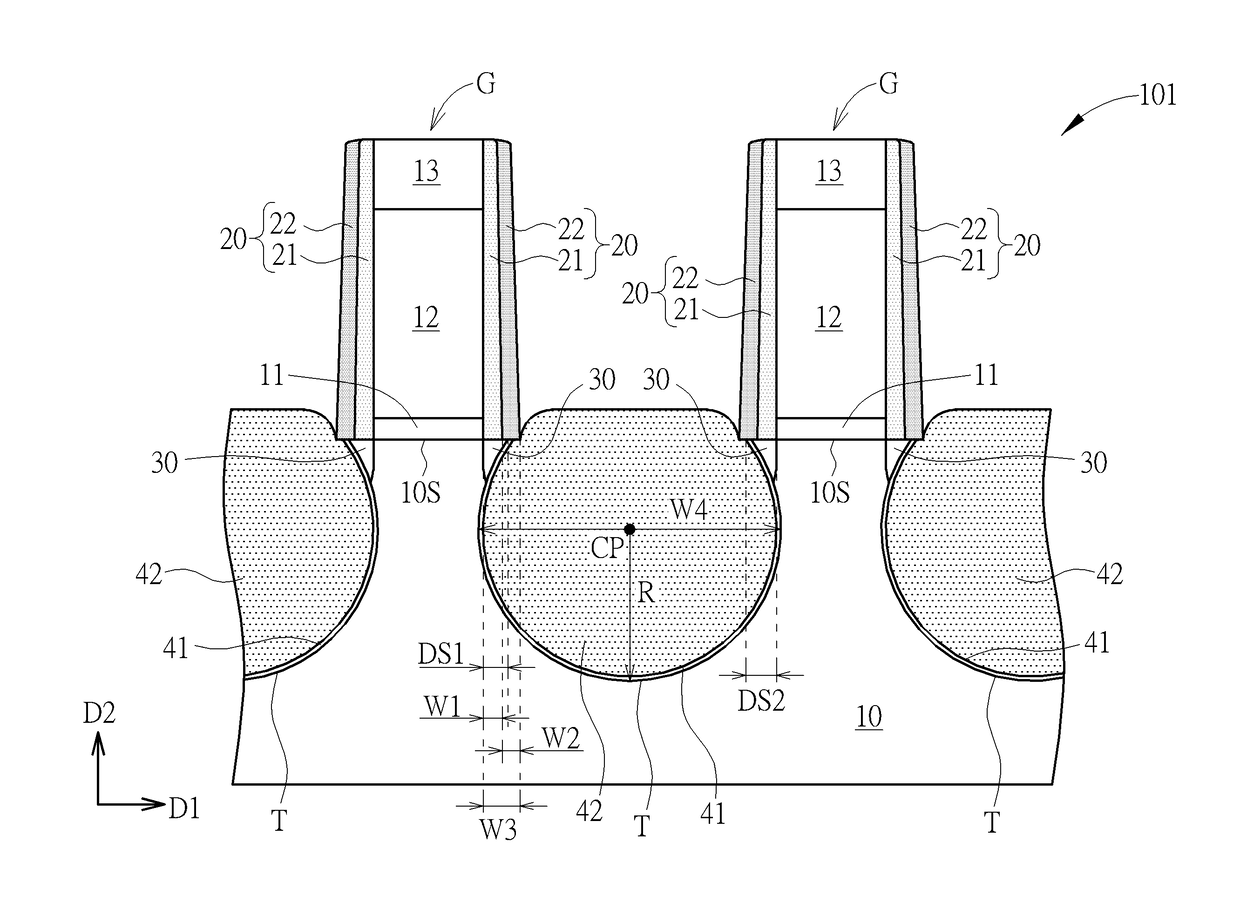
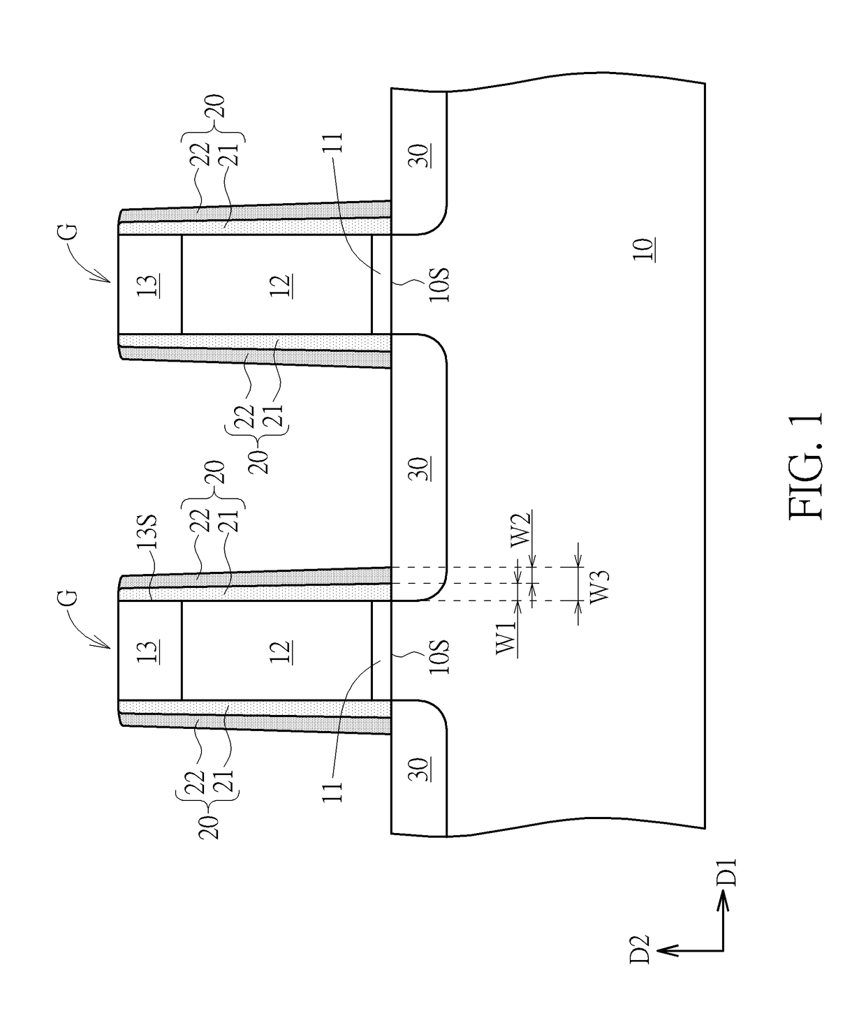
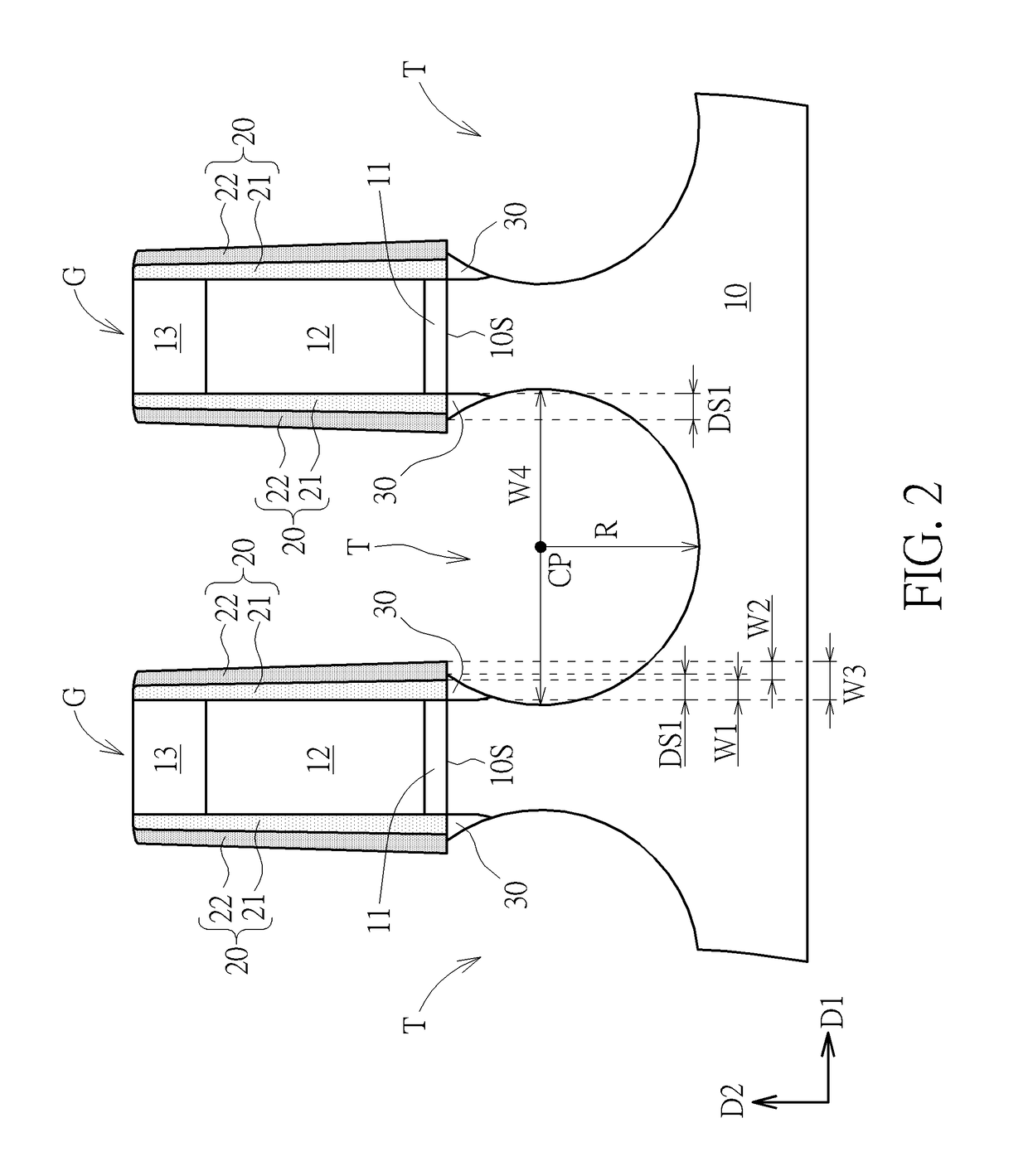
[0017]Please refer to FIGS. 1-3. F FIGS. 1-3 are schematic drawings illustrating a manufacturing method of a semiconductor structure according to a first embodiment of the present invention. The manufacturing method of the semiconductor structure in this embodiment includes the following steps. As shown in FIG. 1, a substrate 10 is first provided, and at least one gate structure G is formed on the substrate 10. In this embodiment, the formation of the gate structure G could be accomplished by sequentially forming a gate dielectric layer, a gate material layer, and a hard mask layer on the substrate 10, conducting a pattern transfer process by using a patterned resist (not shown) as mask to partially remove the hard mask layer, the gate material layer, and the gate dielectric layer through single or multiple etching processes, and stripping the patterned resist for forming at least one gate structure G on the substrate 10. Preferably, each gate structure G is composed of a patterned ...


PUM


Abstract

A semiconductor device includes a substrate, a gate structure, a sidewall spacer, and an epitaxial layer. The gate structure is disposed on the substrate, and the substrate has at least one recess disposed adjacent to the gate structure. The sidewall spacer is disposed on at least two sides of the gate structure. The sidewall spacer includes a first spacer layer and a second spacer layer, and the first spacer layer is disposed between the gate structure and the second spacer layer. The epitaxial layer is disposed in the recess, and the recess is a circular shaped recess. A distance between an upmost part of the recess and the gate structure is less than a width of the sidewall spacer.

Description

BACKGROUND OF THE INVENTION[0001]1. Field of the Invention[0002]The present invention relates to a semiconductor device, and more particularly, to a semiconductor device including a circular shaped recess with a relatively smaller distance between the recess and a corresponding gate structure for improving the performance of the semiconductor device.[0003]2. Description of the Prior Art[0004]In order to increase the carrier mobility of semiconductor structure, it has been widely used to apply tensile stress or compressive stress to a gate channel. For instance, if a compressive stress were to be applied, it has been common in the conventional art to use selective epitaxial growth (SEG) technique to form epitaxial structure such as a silicon germanium (SiGe) epitaxial layer in a silicon substrate. As the lattice constant of the SiGe epitaxial layer is greater than the lattice constant of the silicon substrate thereby producing stress to the channel region of a PMOS transistor, the ca...

Claims


Application Information

Patent Timeline
Patent Type & Authority Applications(United States)
IPC IPC(8): H01L29/78H01L27/088H01L29/08H01L29/06H01L29/165
CPCH01L29/7848H01L29/0688H01L27/088H01L29/0847H01L29/165H01L21/823425H01L21/823814H01L29/161H01L29/6656H01L29/66636H01L29/7834
Inventor SHEN, WEN-JIUNLIU, CHIA-JONGCHANG, CHUNG-FUWU, YEN-LIANGLU, MAN-LINGCHANG, I-FANCHEN, YI-WEI
Owner UNITED MICROELECTRONICS CORP
Why Eureka
Try Eureka