Manufacturing method of gate dielectric layer

a manufacturing method and dielectric layer technology, applied in the direction of basic electric elements, electrical apparatus, semiconductor devices, etc., can solve the problems of affecting device performance, the gate dielectric layer formed with the method above fails to meet the quality demand for and the dielectric constant of the gate dielectric layer decreases, etc., to achieve high quality

Inactive Publication Date: 2012-10-25
NAN YA TECH
View PDF3 Cites 2 Cited by
  • Summary
  • Abstract
  • Description
  • Claims
  • Application Information

AI Technical Summary

Benefits of technology

[0007]The invention is directed to a manufacturing method of a gate dielectric layer. T

Problems solved by technology

However, in the aforementioned annealing treatment, a portion of nitrogen in the nitride layer usually diffuses to the external environment which leads to a decrease in the dielectric constant of the gate dielectric layer.
Additionally, the gate d

Method used


Image

  • Manufacturing method of gate dielectric layer
  • Manufacturing method of gate dielectric layer
  • Manufacturing method of gate dielectric layer

Examples


Embodiment Construction

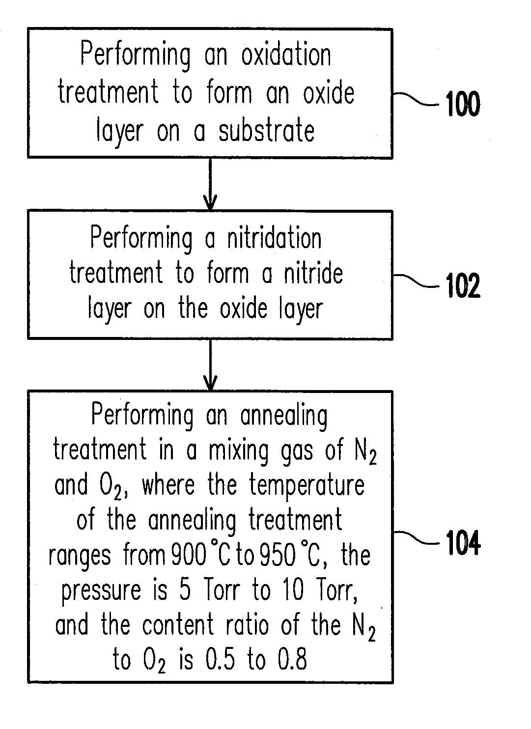
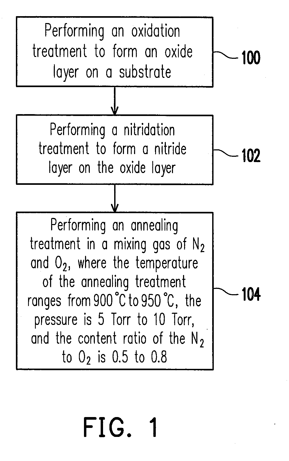
[0019]FIG. 1 illustrates a flow chart for fabricating a gate dielectric layer in one embodiment of the invention. Referring in FIG. 1, in step 100, an oxidation treatment is performed to a substrate to form an oxide layer on the substrate. The substrate is, for example, a silicon substrate. The oxidation treatment includes performing an in-situ steam generation (ISSG) process, for instance. The oxide layer formed has a thickness less than 25 angstrom, for example.

[0020]Afterwards, in step 102, a nitridation treatment is performed to form a nitride layer on the oxide layer. The nitridation treatment includes, for example, performing a decoupled plasma nitridation process. As commonly known by persons skilled in the art, the nitridation treatment is usually a low-temperature treatment. In order to enhance the stability of the layer formed, a thermal treatment is further carried out after the nitridation treatment.

[0021]In step 104, an annealing treatment is performed in a mixing gas o...


PUM


Abstract

A manufacturing method of a gate dielectric layer is provided. An oxidation treatment is performed to form an oxide layer on a substrate. A nitridation treatment is performed to form a nitride layer on the oxide layer. An annealing treatment is performed in a mixing gas of N2 and O2, where the temperature of the annealing treatment is 900° C. to 950° C., the pressure of the annealing treatment is 5 Torr to 10 Torr, and the content ratio of the N2 to O2 is 0.5 to 0.8.

Description

BACKGROUND OF THE INVENTION[0001]1. Field of the Invention[0002]The invention related to a manufacturing method of a dielectric layer and more particularly to a manufacturing method of a gate dielectric layer.[0003]2. Description of Related Art[0004]As the size of metal-oxide-semiconductor (MOS) transistors reduces gradually, the quality required for gate dielectric layers in MOS transistors becomes higher, and the demand for the interface characteristic between the gate dielectric layer and the substrate increases especially.[0005]In the current gate dielectric layer fabrication, an oxidation treatment is usually performed to a substrate first to form an oxide layer on the substrate. Afterwards, a nitridation treatment is performed to form a nitride layer on the oxide layer. An annealing treatment is then performed in N2 to stabilize characteristics of the layer formed. The oxide layer and the nitride layer then constitute a gate dielectric layer.[0006]However, in the aforementione...

Claims


Application Information

Patent Timeline
IPC IPC(8): H01L21/316
CPCH01L29/518H01L21/28229
Inventor SU, KUO-HUICHEN, YI-NANLIU, HSIEN-WEN
Owner NAN YA TECH
Why Eureka
Try Eureka