High density trench MOSFET with single mask pre-defined gate and contact trenches

a high-density, mosfet technology, applied in the direction of basic electric elements, electrical equipment, semiconductor devices, etc., can solve the problems of complex implementation, uneven spacing of spacers, and mask overlays

Inactive Publication Date: 2010-08-03
ALPHA & OMEGA SEMICON INC
View PDF5 Cites 25 Cited by
  • Summary
  • Abstract
  • Description
  • Claims
  • Application Information

AI Technical Summary

Benefits of technology

[0013]As shown in FIG. 2C, a gate trench mask 212, e.g., a patterned layer of a resist, such as a photoresist, may be deposited and patterned on top of the hard mask 204. The gate trench mask 212 includes openings at the gate trenches 208 and gate contact trenches 210 with the openings being larger than the dimensions of the trenches 208, 210. The remaining portions of the gate trench mask 212 cover the body contact trenches 206 to protect them during a subsequent etch step. As shown in FIG. 2D, the trenches 208 and 210 are then simultaneously etched deeper into the semiconductor substrate 202 to a second predetermined depth. Because the openings in the gate trench mask 212 have wider widths wmo than the widths wt of the corresponding trenches, and because the hard mask 204 has already predefined all trench locations the gate trench mask 212 can have a relatively large alignment budget. As a result, overlay issues may be made much more manageable than in the prior art. The openings may be made wide since the edges of the trenches 208, 210 are protected during etching by the hard mask 204. In general, the mask openings may be made as wide as desired, provided that they do not expose body contact trenches 206 to undesired etching.
[0018]As shown in FIG. 2H, a gate trench mask 220, e.g., a photoresist, may be deposited and patterned on top of the hard mask 204. The gate trench mask 220 includes openings at the locations of the gate trench 208 and the gate contact trench 210. The conductive material 218 forming the gate 209, and gate contact 211 and portions of the sidewalls of the trenches 208 and 210 that are not covered by the conductive material 218 may optionally be implanted with suitable dopant species 222, such as Arsenic (As), Phosphorus (P), or Boron (B). The dopants 222 may be implanted perpendicular or at an oblique angle, e.g., 85 degrees, relative to the substrate surface, so that dopants may be implanted into the sidewalls of the trenches 208, 210. Angled dopant implantation into sidewalls of the trenches may provide a more consistent control of channel resistance and device threshold voltage.

Problems solved by technology

However, a mask overlay issue occurs when two masks 102 and 104 are used to form a vertical MOSFET structure because a well controlled spacing between the gate trench and nearby contact trench is required for high density MOSFET devices, which have increasingly smaller dimensions.
However, these proposed schemes, which use various constructs of alternating oxide and nitride blocking planar or sidewall spacers to create a contact trench that is self-aligned to the gate trench, are complicated to implement.
In addition, the spacers may have uniformity problems, wherein spacers at the wafer center may be thicker or thinner than those at the wafer edge.

Method used


Image

  • High density trench MOSFET with single mask pre-defined gate and contact trenches
  • High density trench MOSFET with single mask pre-defined gate and contact trenches
  • High density trench MOSFET with single mask pre-defined gate and contact trenches

Examples


Embodiment Construction

[0009]Although the following detailed description contains many specific details for the purposes of illustration, anyone of ordinary skill in the art will appreciate that many variations and alterations to the following details are within the scope of the invention. Accordingly, the exemplary embodiments of the invention described below are set forth without any loss of generality to, and without imposing limitations upon, the claimed invention.

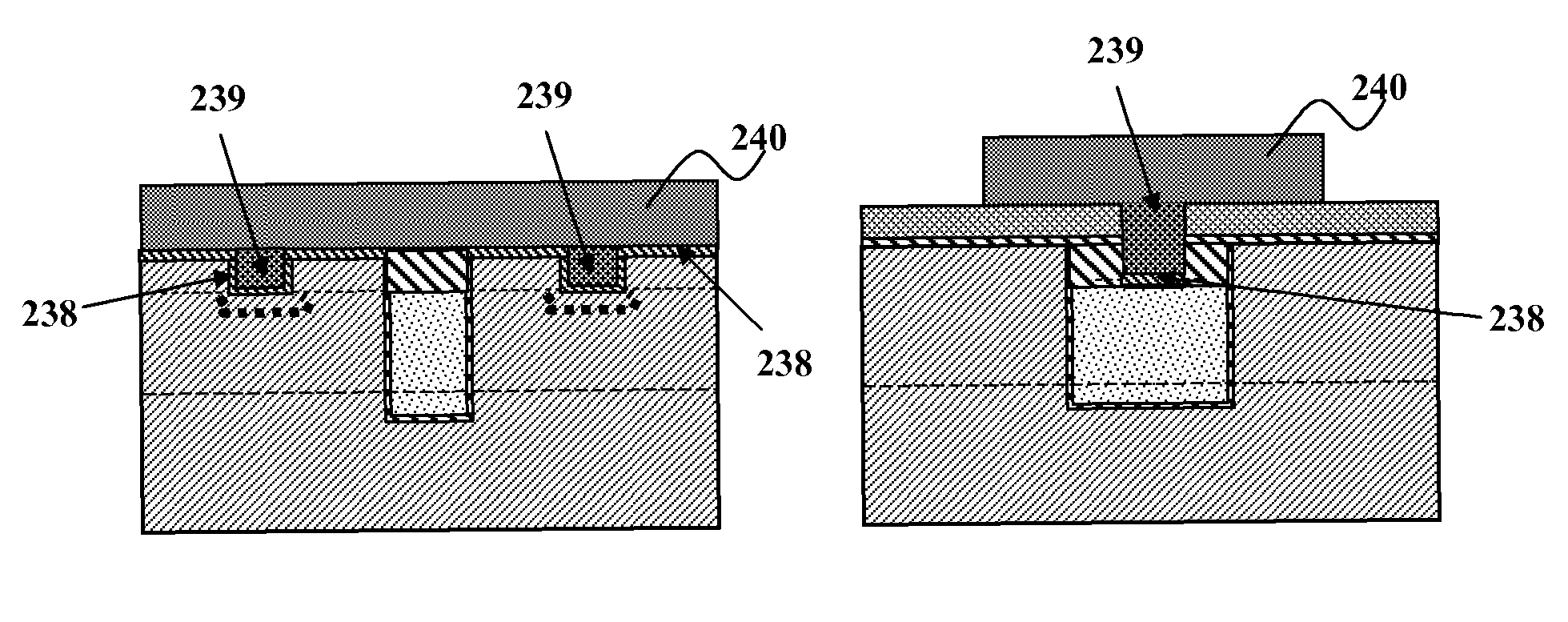
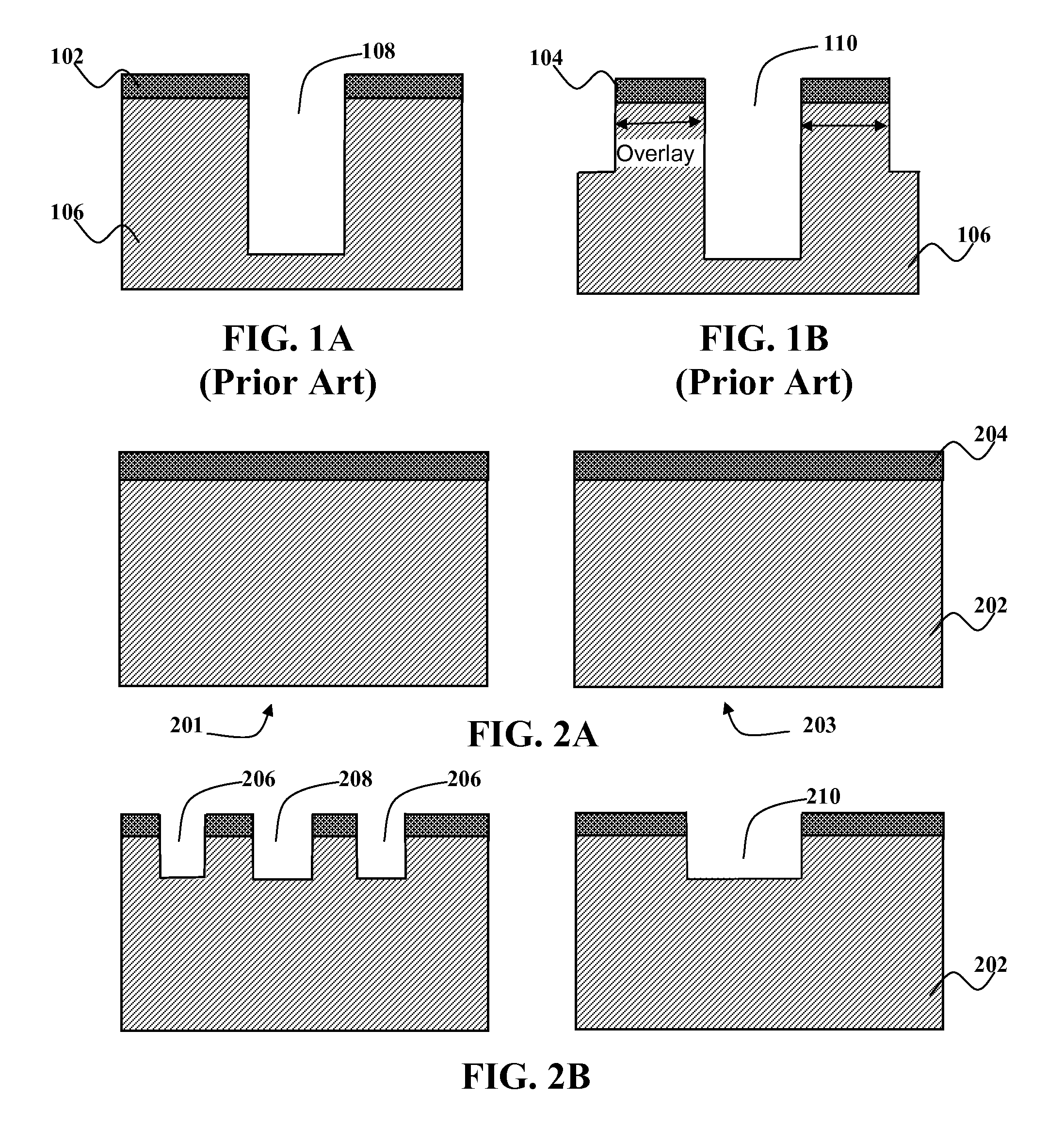
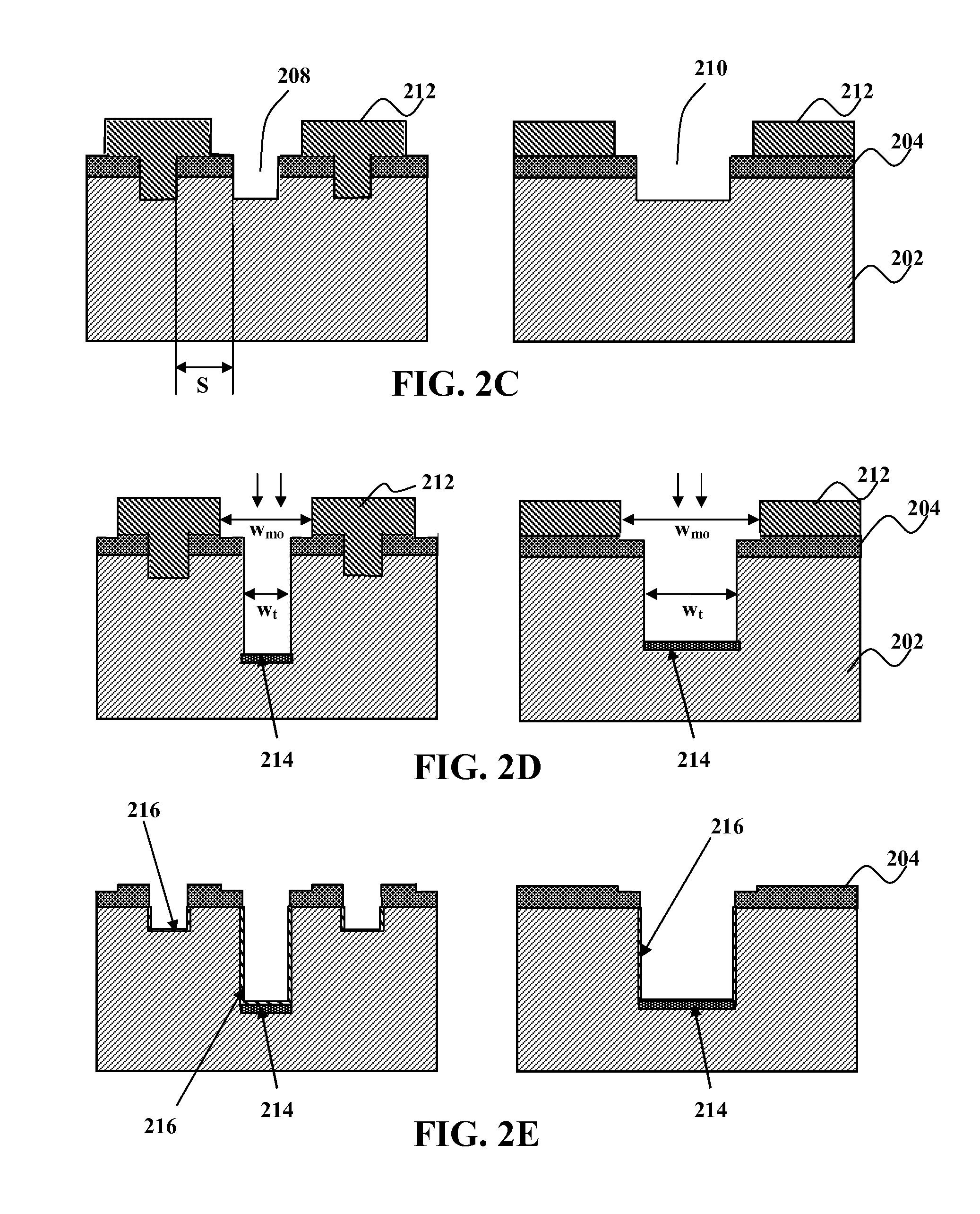
[0010]Embodiments of the present invention present a process that uses a single mask to define both gate and contact trenches without utilizing complicated multiple spacer approaches. An example of a fabrication process according to an embodiment of the present invention is shown in FIGS. 2A-2T.

[0011]The process uses a semiconductor substrate 202 as a starting material. The substrate 202 may be divided into multiple die. Each die may include an active cell area 201 and a gate pickup / contact area 203 at the periphery of a die as shown in FIG....


PUM


Abstract

Trench gate MOSFET devices may be formed using a single mask to define gate trenches and body contact trenches. A hard mask is formed on a surface of a semiconductor substrate. A trench mask is applied on the hard mask to predefine a body contact trench and a gate trench. These predefined trenches are simultaneously etched into the substrate to a first predetermined depth. A gate trench mask is next applied on top of the hard mask. The gate trench mask covers the body contact trenches and has openings at the gate trenches that are wider than those trenches. The gate trench, but not the body contact trench, is etched to a second predetermined depth. Conductive material of a first kind may fill the gate trench to form a gate. Conductive material of a second kind may fill the body contact trench to form a body contact.

Description

FIELD OF THE INVENTION[0001]This invention generally relates to high density trench MOSFET devices and more particularly to a method for making gate and contact trenches of the MOSFET devices with a single mask.BACKGROUND OF THE INVENTION[0002]A MOSFET transistor that includes a trench gate structure offers important advantages over a planar transistor for high current, low voltage switching applications. A trench gate of a MOSFET device typically includes a trench extending from the source to the drain and having sidewalls and a floor that are each lined with a layer of thermally grown silicon dioxide. The lined trench is filled with doped polysilicon. The structure of the trench gate allows less constricted current flow and, consequently, provides lower values of specific on-resistance. Furthermore, the trench gate makes possible a decreased cell pitch in an MOSFET channel extending along the vertical sidewalls of the trench from the bottom of the source across the body of the tra...

Claims


Application Information

Patent Timeline
Patent Type & Authority Patents(United States)
IPC IPC(8): H01L21/336
CPCH01L29/78H01L29/66621H01L29/4236H01L21/26586
Inventor LEE, YEEHENGCHANG, HONGLI, TIESHENGCHEN, JOHNBHALLA, ANUP
Owner ALPHA & OMEGA SEMICON INC
Why Eureka
Try Eureka