Method for manufacturing a bipolar junction transistor

a manufacturing method and transistor technology, applied in the field of semiconductor devices, can solve the problems of affecting bjt performance, affecting the performance of the bjt, and causing too much or too little diffusion of dopants,

Inactive Publication Date: 2005-05-03
TEXAS INSTR INC
View PDF9 Cites 0 Cited by
  • Summary
  • Abstract
  • Description
  • Claims
  • Application Information

AI Technical Summary

Benefits of technology

[0010]Other technical advantages are readily apparent to one sk...

Problems solved by technology

A problem with annealing is that too much, or too little, diffusion of dopants occurs depending on the time and temperature of the annealing process.
Depending on the type of BJT being manufactured, an annealing process can cause ...

Method used


Image

  • Method for manufacturing a bipolar junction transistor
  • Method for manufacturing a bipolar junction transistor
  • Method for manufacturing a bipolar junction transistor

Examples


Embodiment Construction

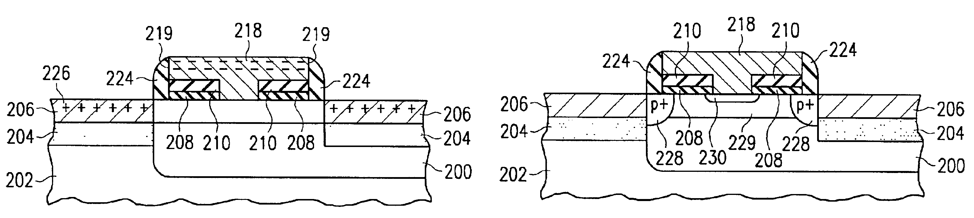
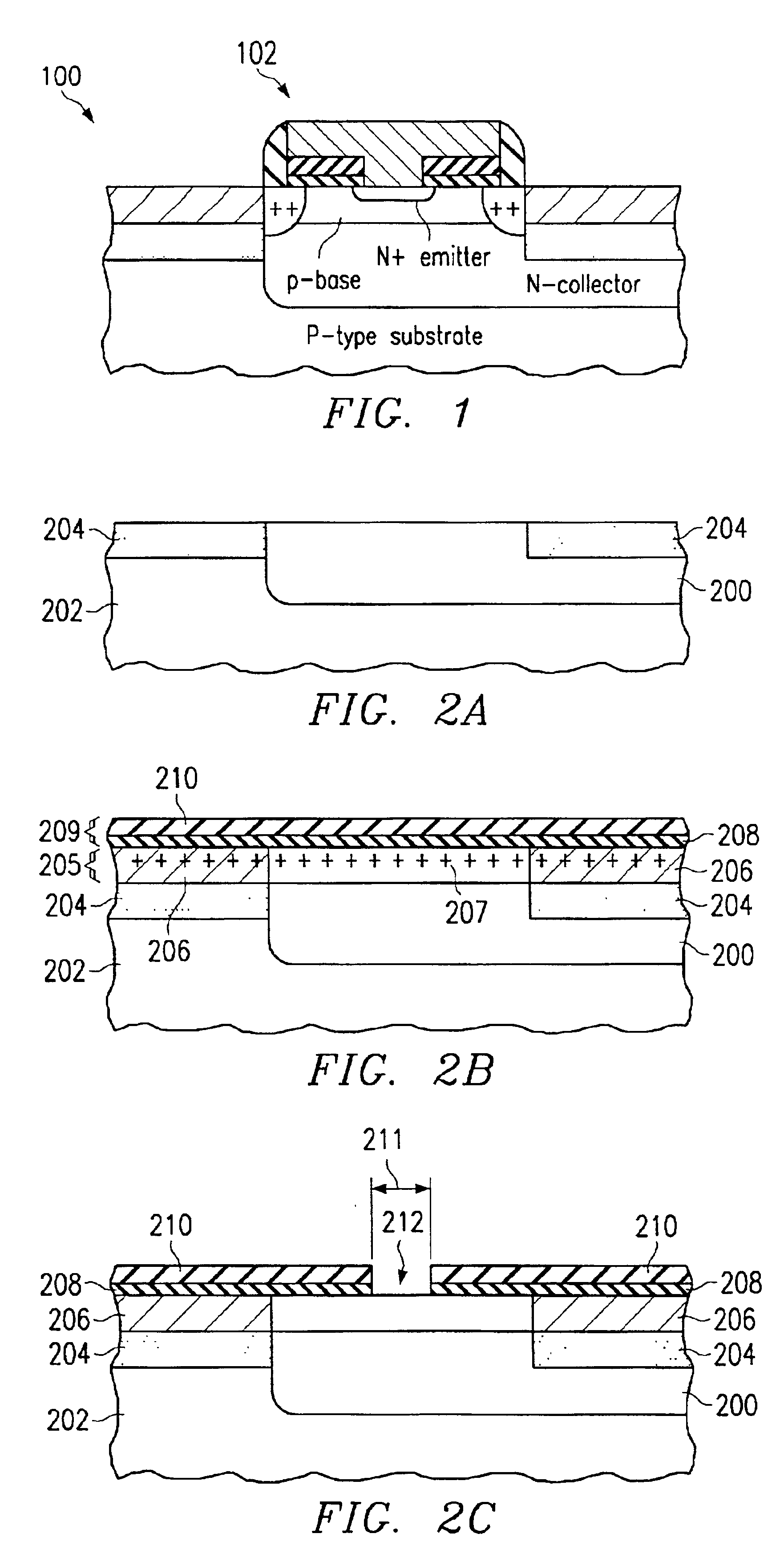
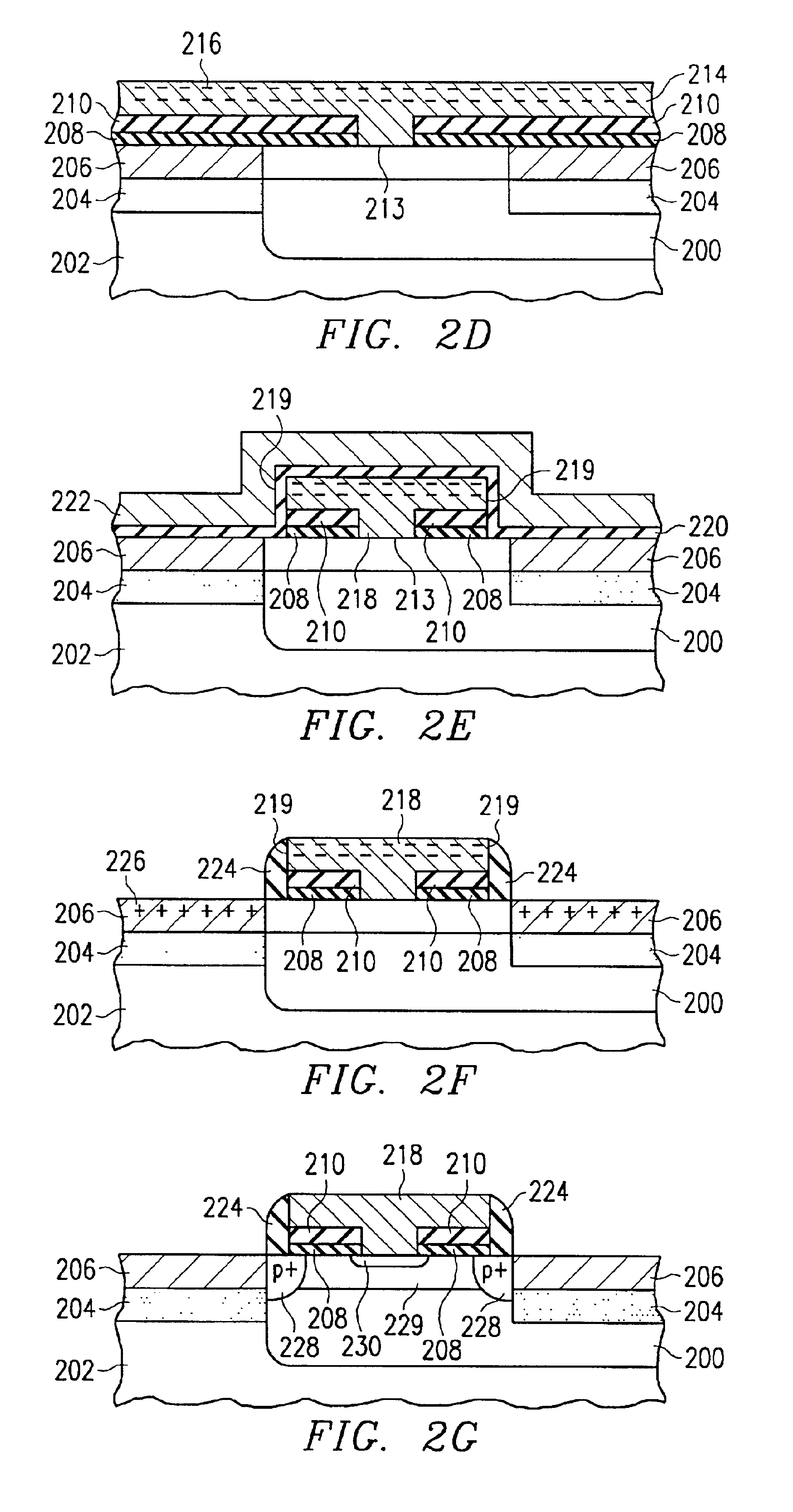
[0016]Example embodiments of the present invention and their advantages are best understood by referring now to FIGS. 1 through 3D of the drawings, in which like numerals refer to like parts.

[0017]FIG. 1 is a cross-sectional view of a partially completed semiconductor device 100 showing a substantially completed bipolar junction transistor (“BJT”) 102 manufactured according to the teachings of the present invention. BJT 102 is shown in FIG. 1 to be a vertical NPN bipolar junction transistor; however, BJT 102 may be formed in other configurations, such as a PNP configuration. Many processes are used in manufacturing bipolar junction transistors; one such process is annealing. An annealing process is a heat treating process that controls, among other things, the formation and diffusion of various dopants in semiconductors. One problem with annealing is that too much, or too little, diffusion of dopants occurs depending on the time and temperature of the annealing process. Depending on...


PUM


Abstract

According to one embodiment of the invention, a method used in manufacturing an intermediate structure in a bipolar junction transistor includes implanting a base dopant in a semiconductor substrate to form a base, forming a dielectric layer outwardly from the semiconductor substrate, etching a portion of the dielectric layer to form an emitter region, forming an emitter polysilicon layer on the semiconductor substrate, and after forming the emitter polysilicon layer, annealing the semiconductor substrate.

Description

CROSS-REFERENCE TO RELATED APPLICATIONS[0001]This application claims priority under 35 USC § 119(e)(1) of provisional application Ser. No. 60 / 256,775, filed Dec. 19, 2000.[0002]This application is related to a provisional patent application filed on the same date as the instant provisional application, entitled Method For Manufacturing A Bipolar Junction Transistor.TECHNICAL FIELD OF THE INVENTION[0003]This invention relates generally to the field of semiconductor devices and, more specifically, to a method for manufacturing a bipolar junction transistor.BACKGROUND OF THE INVENTION[0004]Semiconductor devices are used for many applications, and one component used extensively in semiconductor devices is a transistor. There are many different types of transistors, including bipolar junction transistors. Bipolar junction transistors (“BJTs”) are used to make other types of transistors and devices, such as a complementary metal oxide semiconductor (“CMOS”), which utilizes NPN and PNP BJT...

Claims


Application Information

Patent Timeline
IPC IPC(8): H01L21/02H01L21/331H01L29/732H01L29/02H01L29/08H01L29/66
CPCH01L29/0804H01L29/7322H01L29/66272
Inventor HOWARD, GREGORY E.PINTO, ANGELO
Owner TEXAS INSTR INC
Why Eureka
Try Eureka