Semiconductor device and driver control method

a technology of semiconductor devices and driver control methods, applied in the direction of logic circuits, pulse techniques, reliability increasing modifications, etc., can solve the problems of not being able to disclose any semiconductor device whose output impedance is disclosed, v characteristic does not always have a linear characteristic, and the window width on the low side becomes narrow. , to achieve the effect of improving a signal transmission characteristi

Active Publication Date: 2010-08-03
LONGITUDE LICENSING LTD
View PDF8 Cites 52 Cited by
  • Summary
  • Abstract
  • Description
  • Claims
  • Application Information

AI Technical Summary

Benefits of technology

[0025]An advantage of some aspects of the invention is to provide a semiconductor device and a driver control method capable of improving a signal transmission characteristic and making a control such that a driver section with a linear I-V characteristic can be adapted to various conditions by providing the driver section with a linear I-V characteristic as a driver section (driver section for driving a data transmission line) of a semiconductor device.

Problems solved by technology

However, since an I-V characteristic of an actual transistor shows a characteristic having a non-saturation region and a saturation region, the I-V characteristic does not always have a linear characteristic.
This causes a problem in that the window width on the low side becomes narrow.
That is, the known technique does not disclose any semiconductor device whose output impedance of a driver section does not need to be made to match the characteristic impedance of a signal line.

Method used


Image

  • Semiconductor device and driver control method
  • Semiconductor device and driver control method
  • Semiconductor device and driver control method

Examples


first embodiment

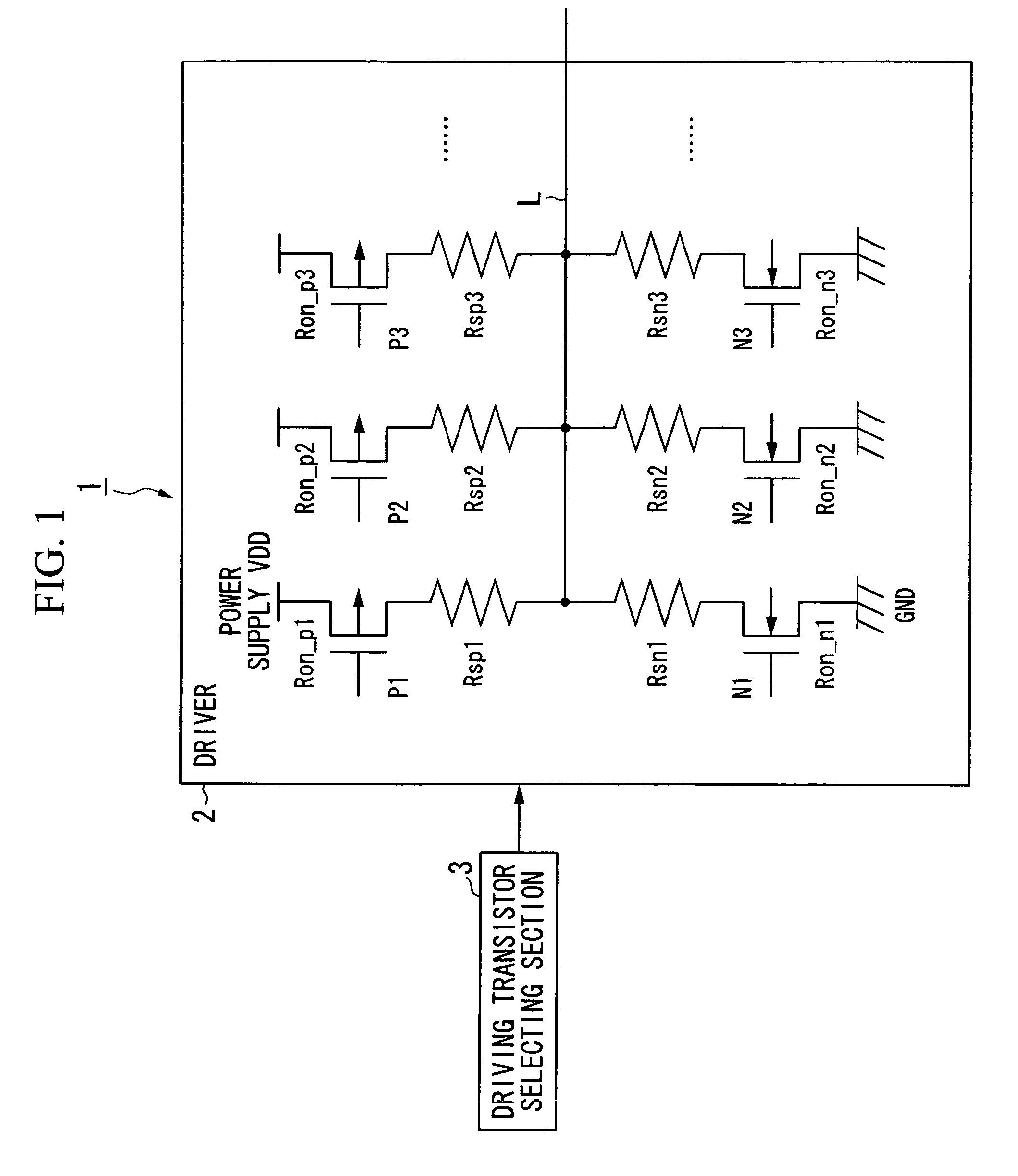
[0044]FIG. 1 is a view showing the configuration of a semiconductor device according to a first embodiment of the invention and is a view showing the configuration of a driver section.

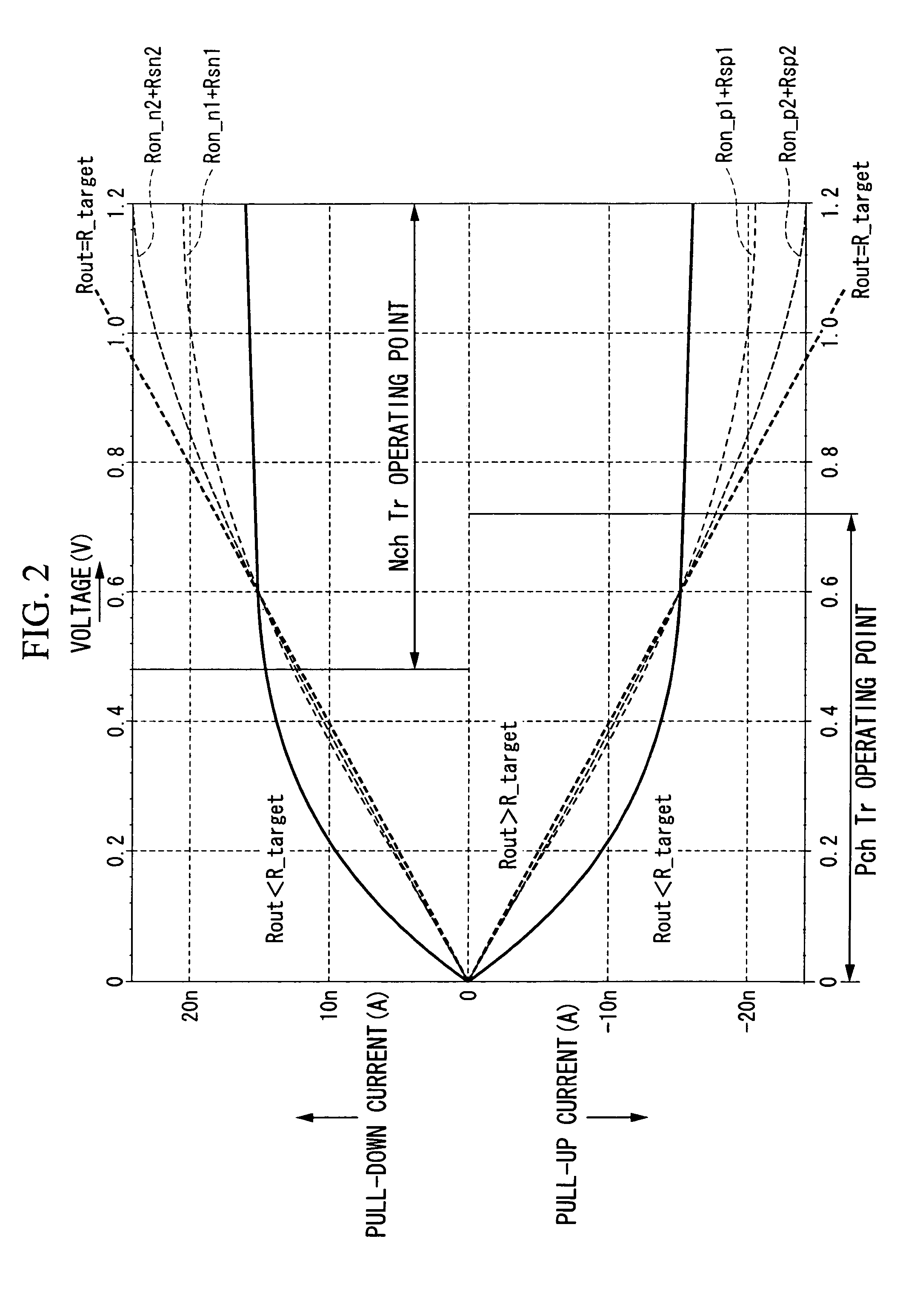
[0045]As shown in FIG. 1, a driver section 1 is configured to include a driver 2 and a driving transistor selecting section 3. The driver 2 is configured to include Pch transistors (Pch MOSFETs) P1, P2, and P3 on the pull-up side and Nch transistors (Nch MOSFETs) N1, N2, and N3 on the pull-down side. The Pch transistors P1, P2, and P3 are Pch transistors having different ON resistance values (may have the same ON resistance value). The Nch transistors N1, N2, and N3 are Nch transistors having different ON resistance values (may have the same ON resistance value).

[0046]Sources of the Pch transistors P1, P2, and P3 on the pull-up side are connected to a power supply VDD, and sources of the Nch transistor N1, N2, and N3 on the pull-down side are connected to the ground (GND).

[0047]A resistance element Rsp...

second embodiment

[0060]FIG. 3 is a view showing the configuration of a semiconductor device according to a second embodiment of the invention and is a view showing the configuration of a driver section.

[0061]A driver section 4 shown in FIG. 3 is configured to include a driver 5, a driving transistor selecting section 6, and a resistance transistor selecting section 7.

[0062]The driver section 4 has Pch transistors (Pch MOSFETs) P1, P2, and P3 (which have different ON resistance values) on the pull-up side and Pch transistors P4, P5 and P6 for selection of resistance elements. The driver section 4 has Nch transistors (Nch MOSFETs) N1, N2, and N3 (which have different ON resistance values) on the pull-down side and Nch transistors N4, N5 and N6 for selection of resistance elements. The Pch transistors P1, P2, and P3 are Pch transistors having different ON resistance values (may have the same ON resistance value). The Nch transistors N1, N2, and N3 are Nch transistors having different ON resistance valu...

third embodiment

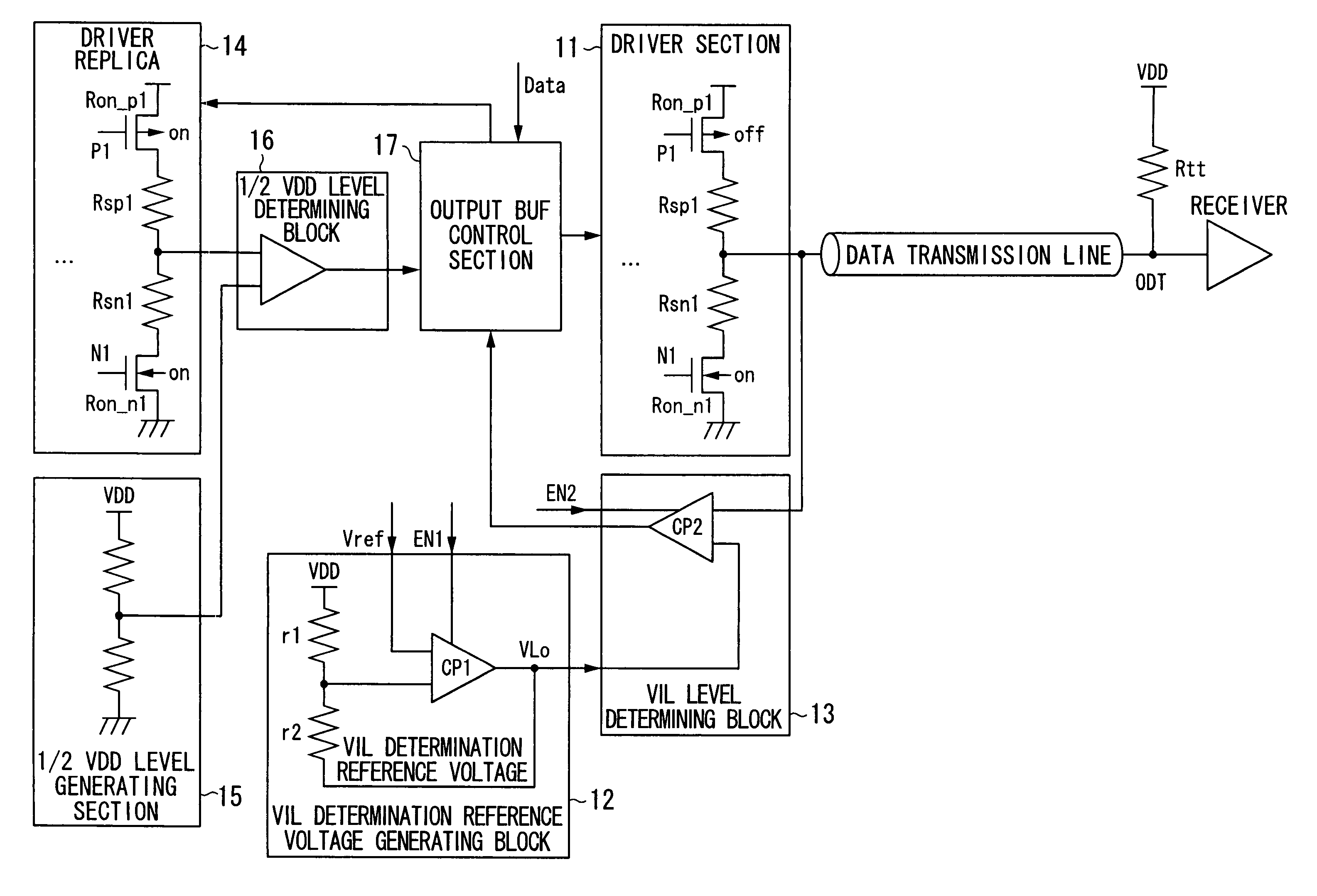
[0077]In the first and second embodiments, examples in which a semiconductor manufacturer suitably selects the optimal combination of transistors and resistance elements from a resistance value of a termination resistor Rtt and the reference voltage VRef value have been described. In a third embodiment of the invention, an example of the configuration having a function of making an adjustment such that the ON resistance of a driver section output becomes optimal will be described.

[0078]A resistance value of the termination resistor Rtt changes with a characteristic impedance of a data transmission line which connects a receiver with a driver section. From a point of view of a reduction in current consumption, there is a case where a termination resistance value is set high in a range in which a problem does not occur even if the waveform quality deteriorates a little.

[0079]The reference voltage VRef depends on the performance of the receiver. In the interface having the same power s...


PUM


Abstract

A semiconductor device of the invention has a plurality of P-channel transistors, to which resistance elements are inserted in series, prepared on a pull-up side of a driver such that an ON resistance value on the P-channel transistor side and a resistance value of the resistance element can be selected. In addition, also on a pull-down side of the driver, a plurality of N-channel transistors to which resistance elements are inserted in series are prepared such that an ON resistance value on the N-channel transistor side and a resistance value of the resistance element can be selected. A driver section having a linear current-voltage characteristic is realized by combination of those described.

Description

BACKGROUND OF THE INVENTION[0001]1. Field of the Invention[0002]The present invention relates to a semiconductor device having a driver section for transmitting data to a data transmission line and a driver control method. In particular, the invention relates to improving a transmission characteristic by providing a driver with a linear current-voltage (I-V) characteristic in the interface having power supply termination (method of pulling up a power supply with a resistor at the end of a transmission line). Furthermore, the invention relates to a semiconductor device which can allow a driver with a linear I-V characteristic to be adapted to various conditions, and a driver section control method.[0003]Priority is claimed on Japanese Patent Application No. 2007-271144, filed Oct. 18, 2007, the content of which is incorporated herein by reference.[0004]2. Description of Related Art[0005]In recent years, there has been a case in which power supply termination of a transmission line is...

Claims


Application Information

Patent Timeline
Patent Type & Authority Patents(United States)
IPC IPC(8): H03K19/094
CPCH03K19/00384H03K19/0005
Inventor HIROSE, YUKITOSHI
Owner LONGITUDE LICENSING LTD
Why Eureka
Try Eureka