Supercharge Your Innovation With Domain-Expert AI Agents!

Method for forming poly-silicon film

a polysilicon film and film technology, applied in the direction of single crystal growth details, crystal growth process, chemistry apparatus and processes, etc., can solve the problems of serious uniformity problems, limited applications of lcd devices with high integrated circuits, and the greatest challenge in manufacturing polysilicon films with large grains and high throughpu

Inactive Publication Date: 2010-08-10
VEGA GRIESHABER GMBH & CO +1
View PDF8 Cites 1 Cited by
  • Summary
  • Abstract
  • Description
  • Claims
  • Application Information

AI Technical Summary

Benefits of technology

The method effectively increases grain size uniformity and carrier mobility, enhancing the electrical characteristics of poly-silicon thin-film transistors and supporting higher integrated circuit applications.

Problems solved by technology

However, the carrier mobility in an amorphous silicon film is much lower than that in a poly-silicon (p-Si) film, so that conventional amorphous silicon TFT-LCDs exhibit low driving current that limits applications for LCD devices with high integrated circuits.
It is thus the greatest challenge to manufacture poly-silicon films having large grains with high throughput.
However, the aforesaid method is only useful when forming a wider poly-silicon grain at the tip of a chevron-shaped region and tends to cause serious uniformity issues.

Method used


Image

  • Method for forming poly-silicon film
  • Method for forming poly-silicon film
  • Method for forming poly-silicon film

Examples


first embodiment

[0051]FIG. 4A and FIG. 4B are top views of optical devices used in a method for forming a poly-silicon film according to the present invention. In FIG. 4A, the optical device 41 (for example, a mask or a micro-slit array) comprises a plurality of first transparent regions 411, each of the first transparent regions 411 having a first periodic shape on an edge region. Alternatively, as shown in FIG. 4B, the optical device 42 (for example, a mask or a micro-slit array) comprises a plurality of first transparent regions 421, each of the first transparent regions 421 having a first periodic shape on each of two opposite edge regions.

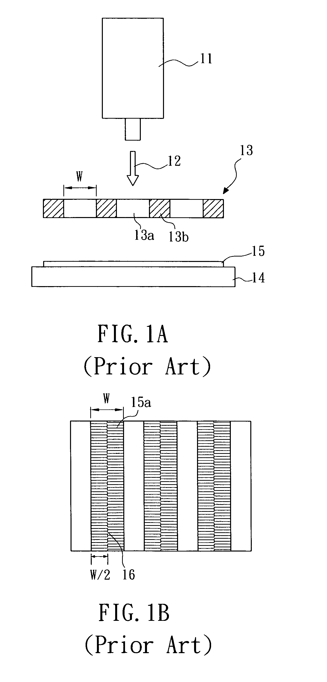
[0052]The transparent regions of a conventional optical device are not provided with a periodic shape on the edge regions. When the melted silicon film is solidified, there are nucleation sites randomly distributed on the silicon film in the regions corresponding to the edge regions. Therefore, the width of poly-silicon grains by conventional SLS is only 0.3˜...

second embodiment

[0061]For example, FIG. 7A and FIG. 7B are top views of masks used in a method for forming a poly-silicon film according to the present invention. In FIG. 7A, the optical device 71 (for example, a mask or a micro-slit array) comprises a plurality of first transparent regions 711 and a plurality of second transparent regions 712 so that the plurality of first transparent regions 711 and the plurality of second transparent regions 712 are arranged in a tier-shape. More particularly, each of the first transparent regions 711 has a first periodic shape on an edge region and each of the second transparent regions 712 has a second periodic shape on an edge region. Alternatively, as shown in FIG. 7B, the optical device 72 (for example, a mask or a micro-slit array) comprises a plurality of first transparent regions 721 and a plurality of second transparent regions 722 so that the plurality of first transparent regions 721 and the plurality of second transparent regions 722 are arranged in ...

third embodiment

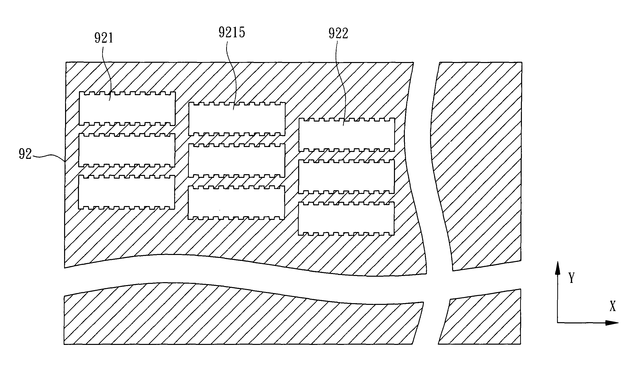
[0073]For example, FIG. 9A and FIG. 9B are top views of masks used in a method for forming a poly-silicon film according to the present invention. In FIG. 9A, the optical device 91 (for example, a mask or a micro-slit array) comprises a plurality of first transparent regions 911, a plurality of second transparent regions 912 and at least a plurality of extended transparent regions 9115. The plurality of extended transparent regions 9115 are disposed between the plurality of first transparent regions 911 and the plurality of second transparent regions 912 so that the plurality of first transparent regions 911, the plurality of extended transparent regions 9115 and the plurality of second transparent regions 912 are arranged in a tier-shape. More particularly, each of the first transparent regions 911 has a first periodic shape on an edge region, each of the second transparent regions 912 has a second periodic shape on an edge region and each of the extended transparent regions 9115 h...


PUM


Abstract

A method for forming a poly-silicon film, using sequential lateral solidification (SLS) by laser irradiation through an optical device to pattern the laser beam and provide a periodic energy profile on the edges of transparent regions so as to widen the poly-silicon grains and achieve grain size uniformity. The optical device comprises a plurality of first transparent regions with a length of L, wherein at least one side of the edge of each of the first transparent regions has a first periodic shape.

Description

BACKGROUND OF THE INVENTION[0001]1. Field of the Invention[0002]The present invention generally relates to a method for forming a poly-silicon (p-Si) film and, more particularly, to a method using sequential lateral solidification (SLS) by laser irradiation through an optical device (for example, a mask or a micro-slit array) to pattern the laser beam and provide a periodic energy profile of the edge of the laser beam passing through the optical device so as to widen the poly-silicon grains and achieve grain size uniformity.[0003]2. Description of the Prior Art[0004]In semiconductor manufacturing, amorphous silicon (a-Si) thin-film transistors (TFTs) are now widely used in the liquid crystal display (LCD) industry because amorphous silicon films can be deposited on a glass substrate at low temperatures. However, the carrier mobility in an amorphous silicon film is much lower than that in a poly-silicon (p-Si) film, so that conventional amorphous silicon TFT-LCDs exhibit low driving ...

Claims


Application Information

Patent Timeline
Patent Type & Authority Patents(United States)
IPC IPC(8): H01L21/00
CPCH01L21/02532H01L21/0268Y10T117/1016
Inventor CHU, FANG-TSUNLIN, JLA-XING
Owner VEGA GRIESHABER GMBH & CO
Features
  • R&D
  • Intellectual Property
  • Life Sciences
  • Materials
  • Tech Scout
  • Unparalleled Data Quality
  • Higher Quality Content
  • 60% Fewer Hallucinations
Learn More