Resistive memory structure with buffer layer

a memory structure and resistive technology, applied in the field of resistive memory structure with buffer layer, can solve the problems of relatively large memory cell size, copper bottom electrode complicating the erasure of memory cells, etc., and achieve the effect of improving performan

Active Publication Date: 2010-08-17
MACRONIX INT CO LTD
View PDF308 Cites 60 Cited by
  • Summary
  • Abstract
  • Description
  • Claims
  • Application Information

AI Technical Summary

Benefits of technology

[0014]Advantageously, the present invention improves the performance, including data retention and cycle endurance, of a resistive memory structure.

Problems solved by technology

This MIM structure requires several additional masks and patterning to form the noble metal electrodes and the memory material, and results in a relatively large memory cell size.
This structure requires several additional masks to form the top and bottom electrodes, and results in a relatively large memory cell size.
Chen et al. disclose that having a copper bottom electrode complicates erasing of the memory cell since the applied field during erasing may push copper ions into the CuxO.

Method used


Image

  • Resistive memory structure with buffer layer
  • Resistive memory structure with buffer layer
  • Resistive memory structure with buffer layer

Examples


Embodiment Construction

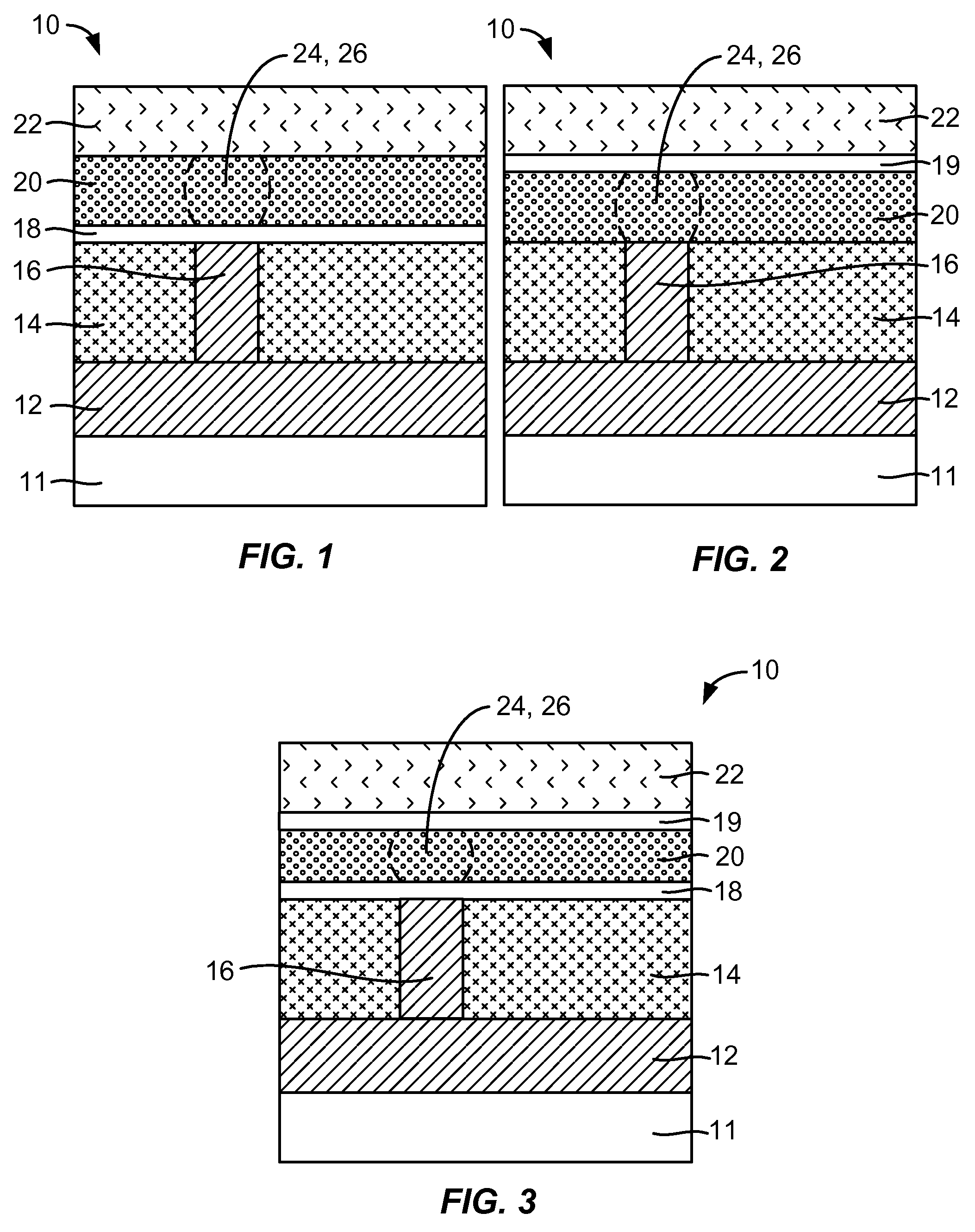
[0026]A description of structural embodiments and methods of the present invention is provided with reference to FIGS. 1-9. It is to be understood that there is no intention to limit the invention to the specifically disclosed embodiments but that the invention may be practiced using other features, elements, methods and embodiments. Like elements in various embodiments are commonly referred to with like reference numerals.

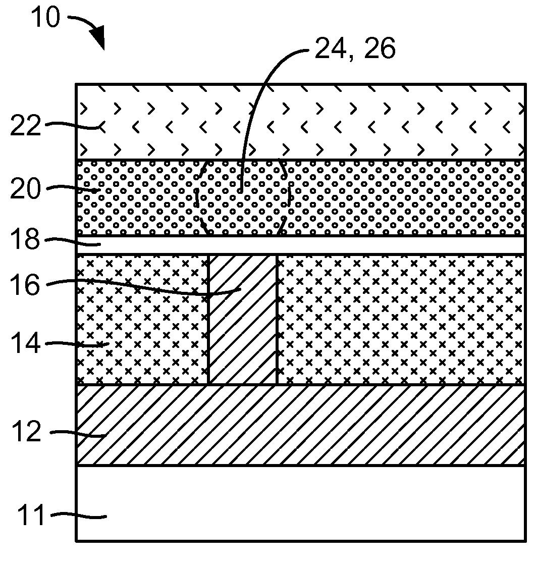
[0027]FIG. 1 is a simplified cross-sectional view of a first example of a resistive memory structure 10. Structure 10 includes a substrate 11 upon which an AlCu stack 12 is formed. A dielectric layer 14, typically silicon dioxide, is formed over stack 12. A bottom electrode 16 extends from stack 12 completely through dielectric layer 14. Bottom electrode 16 is an electrically conductive element. For example, bottom electrode 16 may be a drain terminal of an access transistor or a terminal of a diode. A buffer layer 18 is formed by, for example, down-stream plasma,...


PUM


Abstract

A memory device comprises first and second electrodes with a memory element and a buffer layer located between and electrically coupled to them. The memory element comprises one or more metal oxygen compounds. The buffer layer comprises at least one of an oxide and a nitride. Another memory device comprises first and second electrodes with a memory element and a buffer layer, having a thickness of less than 50 Å, located between and electrically coupled to them. The memory comprises one or more metal oxygen compounds. An example of a method of fabricating a memory device includes forming first and second electrodes. A memory, located between and electrically coupled to the first and the second electrodes, is formed; the memory comprises one or more metal oxygen compounds and the buffer layer comprises at least one of an oxide and a nitride.

Description

CROSS-REFERENCE TO OTHER APPLICATIONS[0001]This application is related to the following U.S. patent applications: Resistance Random Access Memory Structure for Enhanced Retention, application Ser. No. 11 / 560,723, filed 16 Nov. 2006; and Resistance Memory with Tungsten Compound and Manufacturing, application Ser. No. 11 / 955,137, filed 12 Dec. 2007.[0002]This application claims the benefit of U.S. provisional patent application No. 60 / 950,874 filed 20 Jul. 2007.BACKGROUND OF THE INVENTION[0003]1. Field of the Invention[0004]The present invention relates to memory devices and methods for manufacturing high density memory devices, and more particularly to memory devices having a data storage material based on tungsten-oxygen compounds.[0005]2. Description of Related Art[0006]Nonvolatile memory devices include magnetic random access memory MRAM, ferroelectric random access memory FRAM and phase-change random access memory PCRAM and other resistive random access memory RRAM. RRAM has attr...

Claims


Application Information

Patent Timeline
Patent Type & Authority Patents(United States)
IPC IPC(8): H01L47/00
CPCH01L45/04H01L45/06H01L45/085H01L45/12H01L45/1625H01L45/144H01L45/146H01L45/147H01L45/148H01L45/1608H01L45/1233Y10S438/90H10N70/20H10N70/245H10N70/801H10N70/826H10N70/8828H10N70/8833H10N70/8836H10N70/884H10N70/026H10N70/028
Inventor CHIEN, WEI-CHIHCHANG, KUO-PINLAI, ERH-KUNHSIEH, KUANG YEU
Owner MACRONIX INT CO LTD
Why Eureka
Try Eureka