Substrate for electrical device and methods for making the same

a technology for electrical devices and substrates, applied in semiconductor devices, semiconductor/solid-state device details, electrical apparatus, etc., can solve problems such as the failure of electrical devices to function well, and achieve the effects of enhancing the heat dissipation of chips, reducing the restriction on substrate design, and saving costs

Inactive Publication Date: 2010-08-31
WANG CHUNG CHENG
View PDF5 Cites 9 Cited by
  • Summary
  • Abstract
  • Description
  • Claims
  • Application Information

AI Technical Summary

Benefits of technology

[0006]It is therefore an object of the invention to solve the mentioned-above problems, in accordance with the invention, the substrate includes an insulator and a plurality of conductive elements, wherein the conductive elements are embedded in the insulator, and a portion of conductive element exposed to the insulator for external connection, wherein the portion of conductive element exposed to the insulator may protrude the insulator surface for external connection, In this manner, the solder balls are not needed. Moreover, the substrate of the present invention may further comprise a submember serving as a heat spreader which is for enhancing the heat dissipation of chip, In addition, due to the conductive element of substrate is solid and hard enough, in accordance with the present invention, in this manner, the conductive wire enables to be electrically connected to the conductive element directly, then cost is saved and the restriction for designing the substrate is decreased too, moreover, the conductive element of substrate may further including either an extending portion or a protruding portion.

Problems solved by technology

When the peeling-off problem happened, the solder ball 50 separated from the conductive element 8 easily, it may cause the electrical device 9 not to be functional well.

Method used


Image

  • Substrate for electrical device and methods for making the same
  • Substrate for electrical device and methods for making the same
  • Substrate for electrical device and methods for making the same

Examples


first embodiment

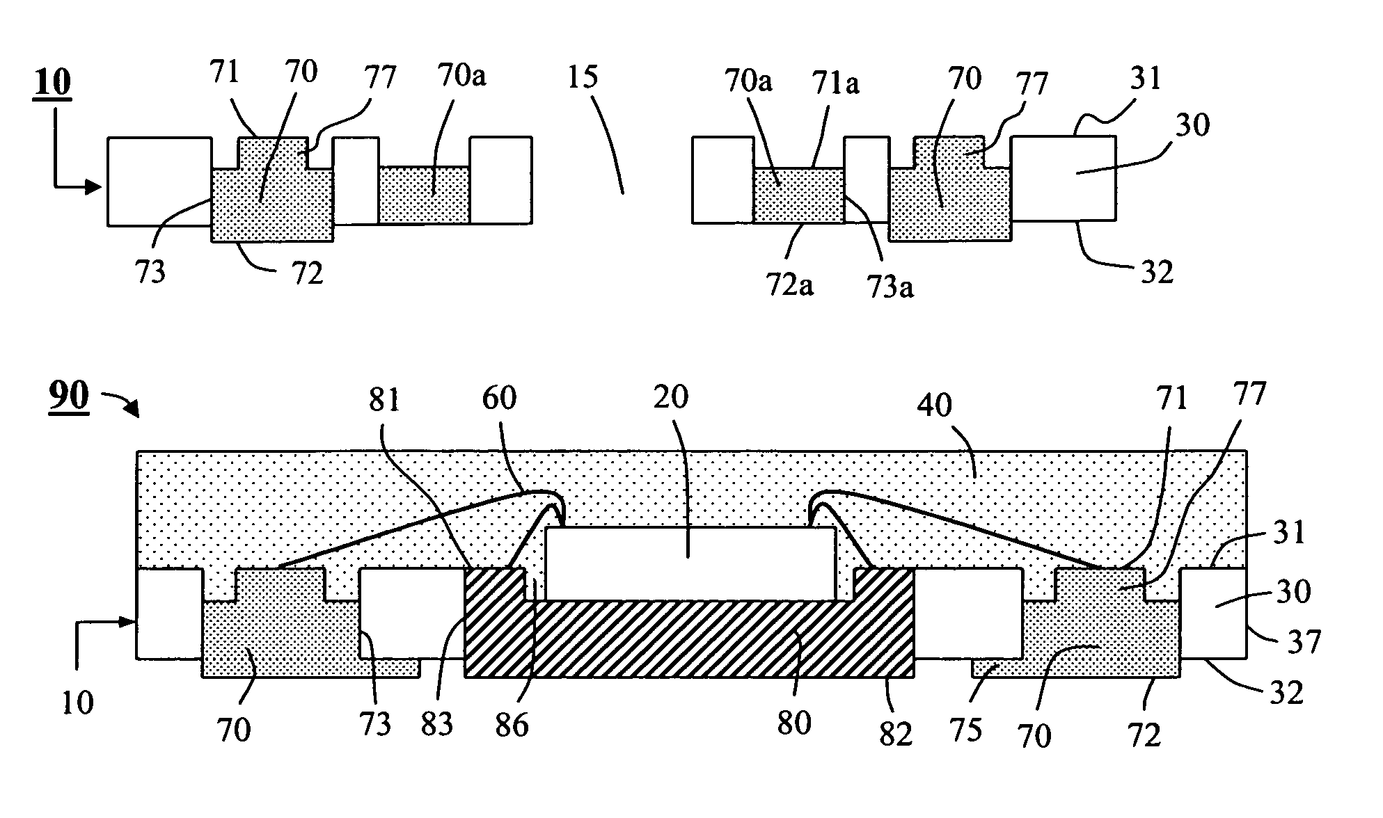
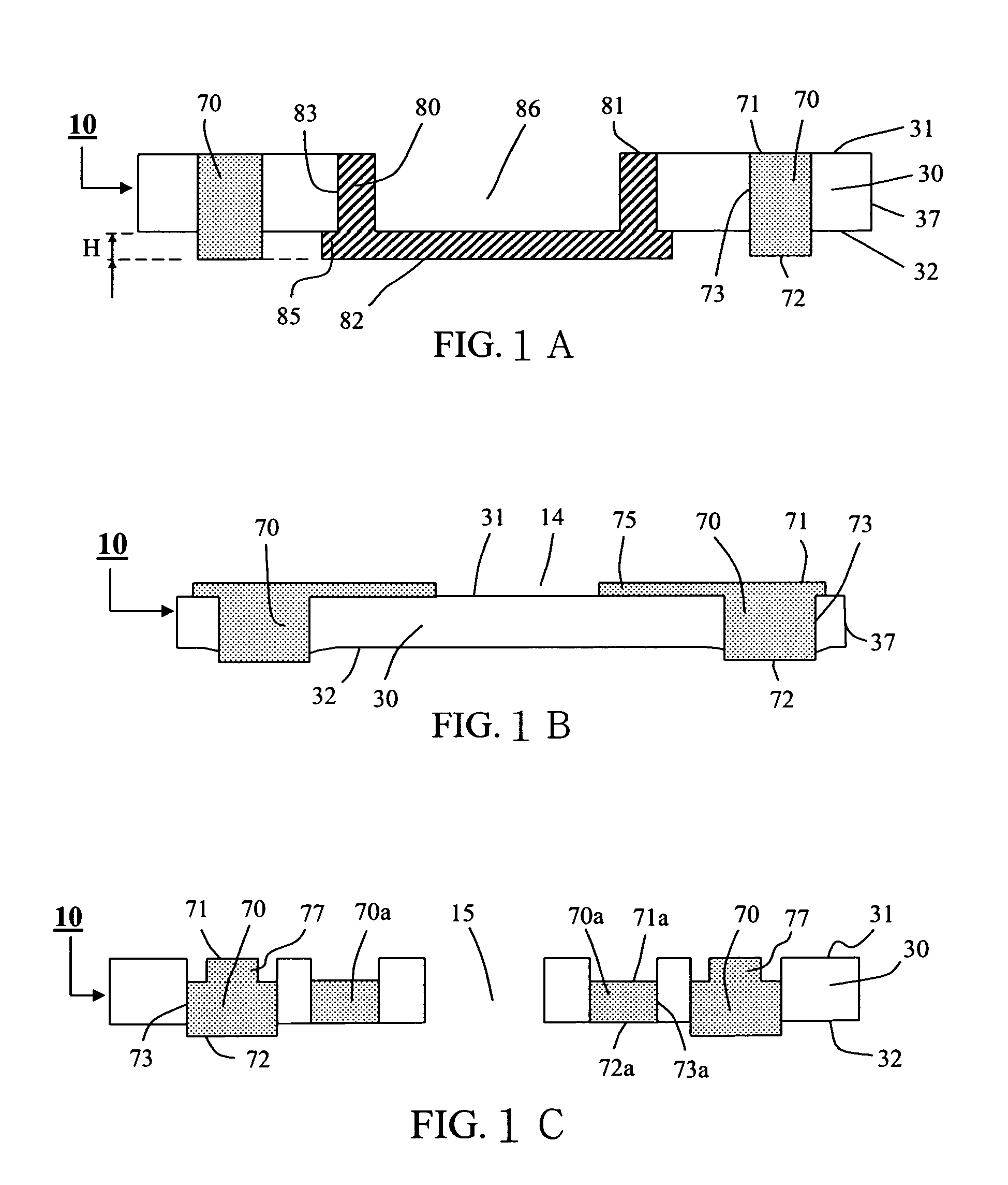
[0028]A first embodiment of substrate of the present invention will be explained with reference to FIG. 1A˜1J, wherein said first embodiment of substrate comprised of an insulator and a plurality of first conductive elements, wherein said first conductive element may include either an extending portion (refer to FIG. 1B) or a protruding portion (refer to FIG. 1C), Moreover, the first embodiment of substrate may also include a submember as required, detailed descriptions as follow:

[0029]FIG. 1A shows a substrate 10 comprising: an insulator 30, said insulator 30 having a first upper surface 31, a first lower surface 32 and a side wall 37; a plurality of first conductive elements 70 which are made of either copper, copper alloy, nickel, aluminum, titanium or metallic alloy, said first conductive elements 70 are substantially solid; said first conductive elements 70 having a first upper surface 71, a first lower surface 72 and a first side edge 73 respectively, each said first side edge...

second embodiment

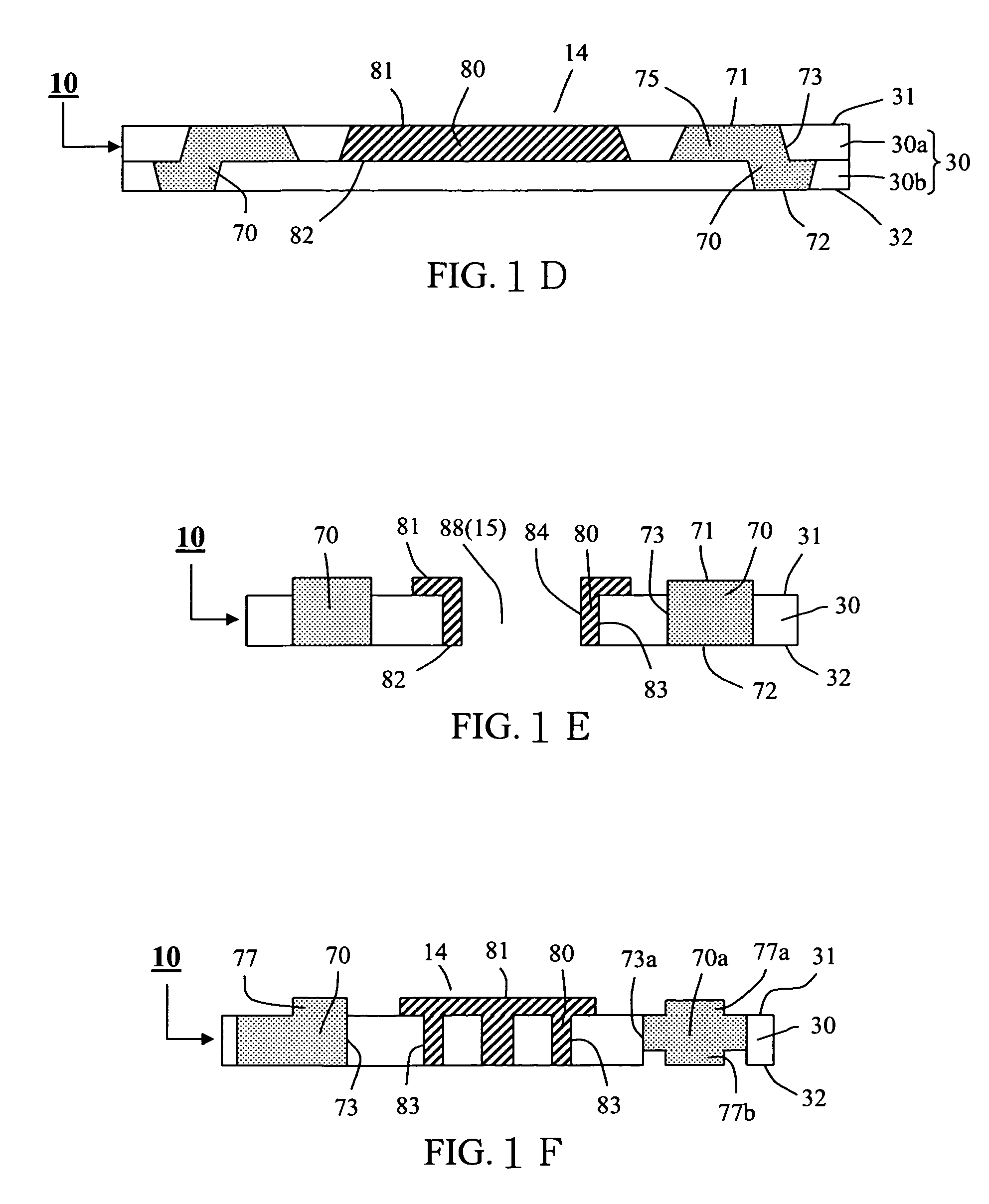
[0039]The second embodiment of present invention will be explained with reference to FIG. 1K˜FIG. 1O, wherein the substrate herein consists of an insulator and two conductive layers which are formed by a plurality of first conductive elements and a plurality of second conductive elements respectively; the first conductive elements are electrically connected to the second conductive elements by a plurality of via and / or conductor respectively, meanwhile, the substrate herein may also be formed by the first embodiment of substrate of the present invention combined with the second conductive elements, moreover, the substrate herein may further include a submember as required; detailed descriptions as follow:

[0040]FIG. 1K shows a substrate 11 comprising: an insulator 30 having a first upper surface 31, a first lower surface 32; a submember 80 such as a heat spreader having a first upper surface 81, a first lower surface 82 and an extending portion 85; a plurality of first conductive ele...

third embodiment

[0045]The third embodiment of substrate of the preset invention will be explained with reference to FIG. 1P and FIG. 1Q, wherein the substrate herein consists of a plurality of insulator and a plurality of conductive layers formed by a plurality of conductive elements respectively, said substrate herein is formed by the first and / or the second embodiment of substrate in accordance with the invention, wherein a plurality of via and / or a plurality of conductor electrically connect each conductive element to the other one respectively, in this manner, the substrate herein is formed to a multi-layer substrate, moreover the substrate herein may also include submember(s) such as heat spreader(s) etc. as required, detail descriptions as follow:

[0046]FIG. 1P shows a substrate 12 which is formed by a substrate 10 which is one of the first embodiments of the present invention associated with a substrate 11 which is one of the second embodiments of the present invention, wherein the substrate ...


PUM


Abstract

Substrate for electrical devices and methods of manufacturing such substrate are disclosed. An embodiment for the substrate comprised of an insulator and a plurality of conductive elements, wherein the conductive elements embedded in the insulator, and two surfaces of the conductive element exposed to two surfaces of the insulator for electrical connection respectively, meanwhile a portion of conductive element may protrude the insulator, in this manner, solder balls are not needed, moreover the conductive element of substrate may further include either an extending portion or a protruding portion, and the present invention may be capable of affording a thinner electrical device thickness, enhanced reliability, and a decreased cost in production.

Description

BACKGROUND OF THE INVENTION[0001]1. Field of the Invention[0002]The present invention generally relates to a substrate for electrical device, and more particularly to a substrate which is enhancing the reliability of electrical device and downsizing an electrical device.[0003]2. Description of the Related Art[0004]Currently, both science and technology are developing rapidly, meanwhile, electrical devices are designed for thinner, wider application, lower cost, and better quality, wherein the better quality of electrical device includes higher reliability and enhanced heat dissipation, in order to achieve above objects, the manufacturers keep on developing it.[0005]FIG. 17 shows a conventional electrical device 9 comprising a substrate 1 which including an insulator 30, a plurality of conductive elements 7,8 and a via 5, wherein said insulator 30 having a first upper surface 31 and a first lower surface 32, said first upper surface 31 of insulator 30 having an receiving area 4 which...

Claims


Application Information

Patent Timeline
Patent Type & Authority Patents(United States)
IPC IPC(8): H01L23/48H01L21/48
CPCH01L23/3121H01L23/3128H01L23/3677H01L23/49805H01L23/49861H01L25/0652H01L2224/48091H01L2224/48227H01L2224/4824H01L2224/49109H01L2924/01046H01L2924/01078H01L2924/01079H01L2924/09701H01L2924/15331H01L2924/19041H01L2924/00014H01L24/48H01L24/49H01L2924/00H01L2224/45099H01L2224/45015H01L2924/207
Inventor WANG, CHUNG-CHENG
Owner WANG CHUNG CHENG
Why Eureka
Try Eureka