Antiferromagnetic half-metallic semiconductor and manufacturing method therefor
a technology of antiferromagnetic semiconductor and half-metallic semiconductor, which is applied in the direction of magnetism bodies, crystal growth process, polycrystalline material growth, etc., can solve the problem that no one has manufactured or proposed a half-metallic antiferromagnet as a spintronic material
- Summary
- Abstract
- Description
- Claims
- Application Information
AI Technical Summary
Benefits of technology
Problems solved by technology
Method used
Image

Examples
first embodiment
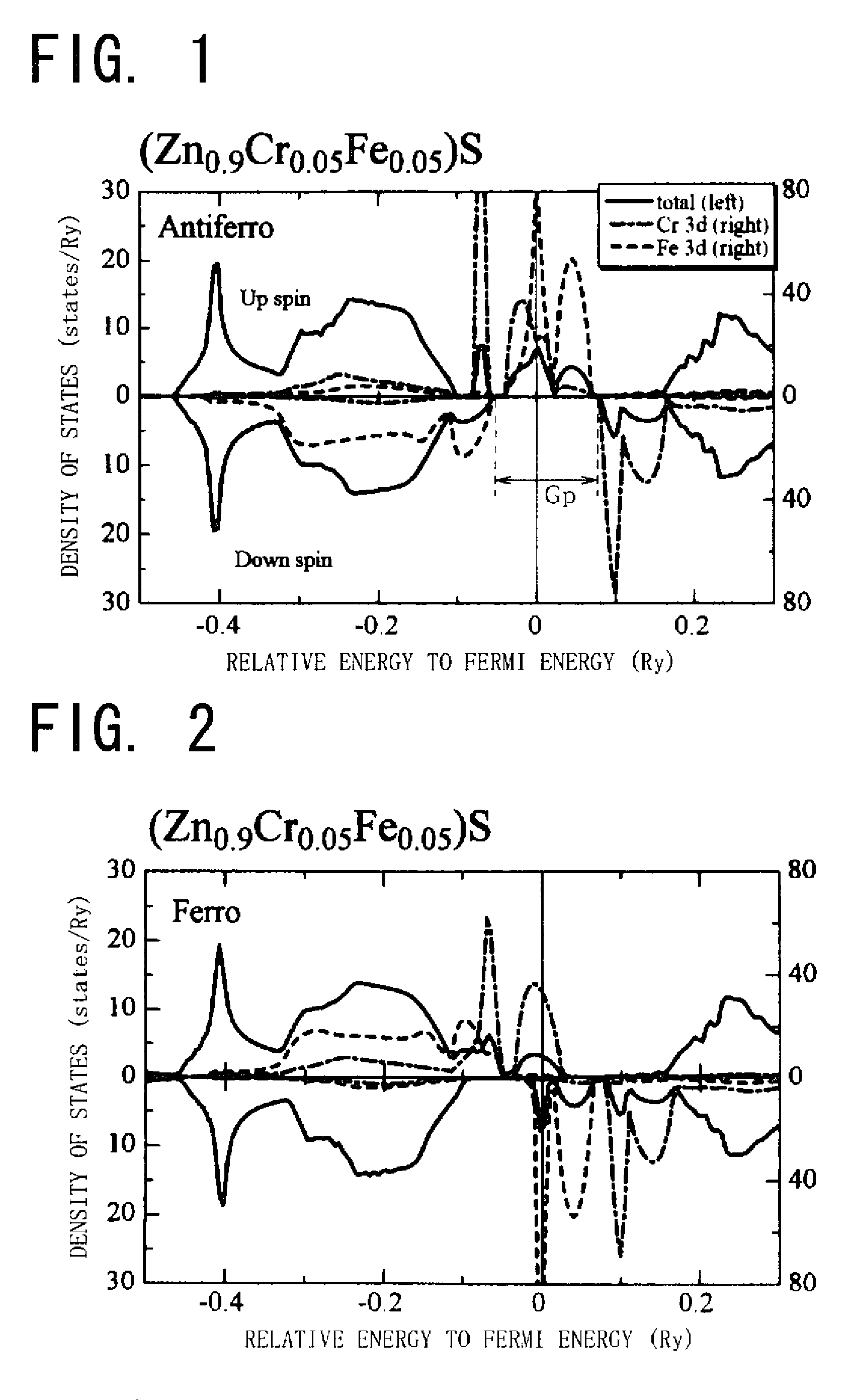
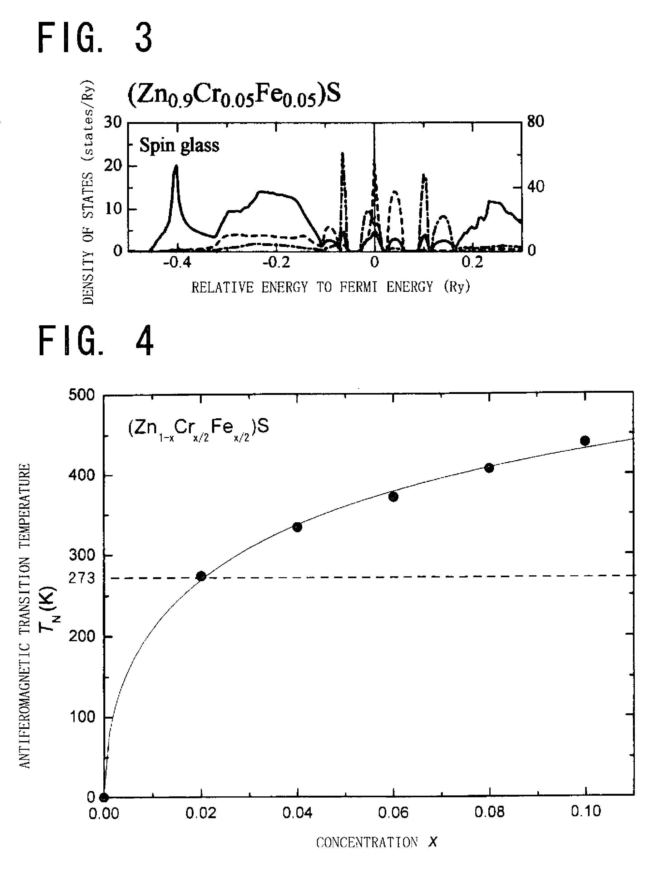
[0061]A diluted antiferromagnetic half-metallic semiconductor of the present embodiment is represented by a composition formula (Zn0.9Cr0.05Fe0.05)S, and has a part of a II element Zn of a II-VI compound semiconductor of ZnS substituted with transition metal elements of Cr and Fe.
[0062]A manufacturing method for the diluted antiferromagnetic half-metallic semiconductor includes growing a ZnS thin film on a GaAs(100) substrate with a laser MBE method, and simultaneously irradiating Cr gas and Fe gas toward the substrate to add 5% each of Cr and Fe. At this time, the substrate temperature is set, for example, to 150-200° C., with a Zn molecular beam having a beam pressure of, for example, 2.5×10⁻⁵ to 8×10⁻⁵ Pa, and an S molecular beam having a beam pressure of, for example, 1.5×10⁻⁴ to 12×10−4 Pa. The gas pressure of Cr and Fe is set, for example, to 2.5×10⁻⁶ to 15×10−6 Pa.
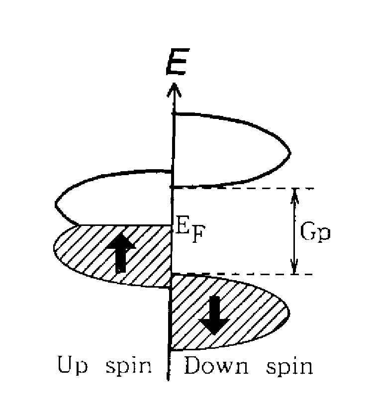
[0063]The present inventors performed first-principles electronic state calculations in order to confirm that the...
second embodiment
[0072]A diluted antiferromagnetic half-metallic semiconductor of the present embodiment is represented by a composition formula (Zn0.9V0.05Co0.05)S, and has a part of a II element Zn of a II-VI compound semiconductor of ZnS substituted with transition metal elements of v and Co.
[0073]A manufacturing method for the diluted antiferromagnetic half-metallic semiconductor includes growing a ZnS thin film on a GaAs(100) substrate with a laser MBE method, and simultaneously adding 5% each of V and Co.
[0074]The present inventors performed first-principles electronic state calculations, as in the first embodiment, in order to confirm that the above manufacturing method exhibits half-metallicity and antiferromagnetism.
[0075]FIG. 5 through FIG. 7 show density-of-states curves in an antiferromagnetic state, a ferromagnetic state and a spin glass state, respectively, obtained by the first-principles electronic state calculations. In the drawings, solid lines represent a total density of states, ...
third embodiment
[0081]A diluted antiferromagnetic half-metallic semiconductor of the present embodiment is represented by a composition formula (Zn0.9Cr0.05Co0.05)O, and has a part of a II element Zn of a II-VI compound semiconductor of ZnO substituted with transition metal elements of Cr and Co.
[0082]A manufacturing method for the diluted antiferromagnetic half-metallic semiconductor includes growing a ZnO thin film on a GaAs(100) substrate with a laser MBE method, and simultaneously adding 5% each of Cr and Co.
[0083]The present inventors performed first-principles electronic state calculations, as in the first embodiment, in order to confirm that the above manufacturing method exhibits half-metallicity and antiferromagnetism.
[0084]FIG. 8 and FIG. 9 show density-of-states curves in an antiferromagnetic state and a spin glass state, respectively, obtained by the first-principles electronic state calculations. In the drawings, solid lines represent a total density of states, one-dot chain lines a lo...
PUM
 Abstract
Description
Claims
Application Information