Control apparatus of semiconductor switch

a control apparatus and semiconductor technology, applied in relays, emergency protective arrangements for limiting excess voltage/current, pulse techniques, etc., can solve the problems of increasing the temperature of the channel of this mosfet ta, increasing the power loss of the mosfet ta, and shortening the judging time. , to achieve the effect of shortening the judging time, increasing the discrimination precision, and quickly cutting off the circui

Inactive Publication Date: 2010-09-07
YAZAKI CORP
View PDF21 Cites 4 Cited by
  • Summary
  • Abstract
  • Description
  • Claims
  • Application Information

AI Technical Summary

Benefits of technology

[0028]The present invention has been made to solve the above-described problems of the related art, and therefore, has an object to provide a control apparatus of a semiconductor switch, capable of increasing discrimination precision between a shortcircuit current and a rush current, and at the same time, capable of shortening a judging time for detecting an occurrence of a shortcircuit current as short as possible. Thus, this control apparatus can quickly cut off a circuit when the shortcircuit current is produced, and thus, can minimize a power loss and a temperature increase of a semiconductor element.
[0042]In accordance with the control apparatus of the semiconductor switch of the present invention, in such a switching circuit that the semiconductor switch is arranged on a high side of a load, when a wiring line for connecting the semiconductor switch to the load is shortcircuited to be grounded, and thus, an excessively large shortcircuit current flows, a judgement is made as to whether or not a magnitude of counter electromotive force E1 generated on a first wiring line for connecting a plus terminal of a power supply to the semiconductor switch exceeds a predetermined value. As a result, the shortcircuit current can be detected within a minimum time just after the shortcircuit current is produced. Thus, a cutoff operation of the shortcircuit current can be urged, so that a power loss which is produced in the semiconductor switch by the shortcircuit current can be suppressed to a minimum power loss.
[0043]As a result, when a semiconductor element which is employed as a switch is selected, limitations caused by a withstanding characteristic with respect to the shortcircuit current may be relaxed. Therefore, semiconductor elements having relatively small capacities may also be employed, which may reduce production cost.
[0045]Furthermore, since an increased gradient of a current which exceeds a rush current is present only in a shortcircuit current, and also, a current increase phenomenon occurred at this time is accompanied with an abrupt large energy change, there is a small possibility as to an erroneous judgement in the judging method employed by the present invention, and therefore, this judging method may have superior reliability.
[0046]Also, the higher the power supply voltage is increased, the larger the destroying energy becomes which is given to the semiconductor element by the shortcircuit current. In the case that a battery of a vehicle is exemplified, a shortcircuit current produced in a 42 V battery series may cause more serious problem, as compared with that of a 12 V battery series. However, in accordance with the present invention, an increase of a current when a shortcircuit current is produced, and a duration time of the increased current can be theoretically minimized, as compared with those of the related method. As a result, even in a high voltage battery series such as a 42 V battery series, the control apparatus of the semiconductor element may be employed as a unit capable of protecting a semiconductor element from a shortcircuit current, which is employed on a high potential side of a load.

Problems solved by technology

If a large current flows under this condition, then a power loss of the MOSFET TA is increased.
In the case of FIG. 10, since the current ID is increased after the present time has passed through the point B2, the power loss of the MOSFET TA becomes large value, which may cause a temperature of the channel of this MOSFET TA to be increased.
In other words, such an element having a small chip size cannot be used, so that a design freedom is restricted, which may cause a cost-up factor.
Also, there is another problem in fluctuations of the reference current Iref.
Any of these solving methods may cause the cost-up factor.
Similarly, this solving method may cause the cost-up factor.
As a result, when the peak value of the rush current is increased, the time required to be reached to the judging value is prolonged, so that the judgement as to the occurrence of the shortcircuit is delayed, and therefore, the timing when the shortcircuit current is cut off is delayed.
As a consequence, the power loss of the semiconductor element is increased, so that such a problem may occur.

Method used


Image

  • Control apparatus of semiconductor switch
  • Control apparatus of semiconductor switch
  • Control apparatus of semiconductor switch

Examples


second embodiment

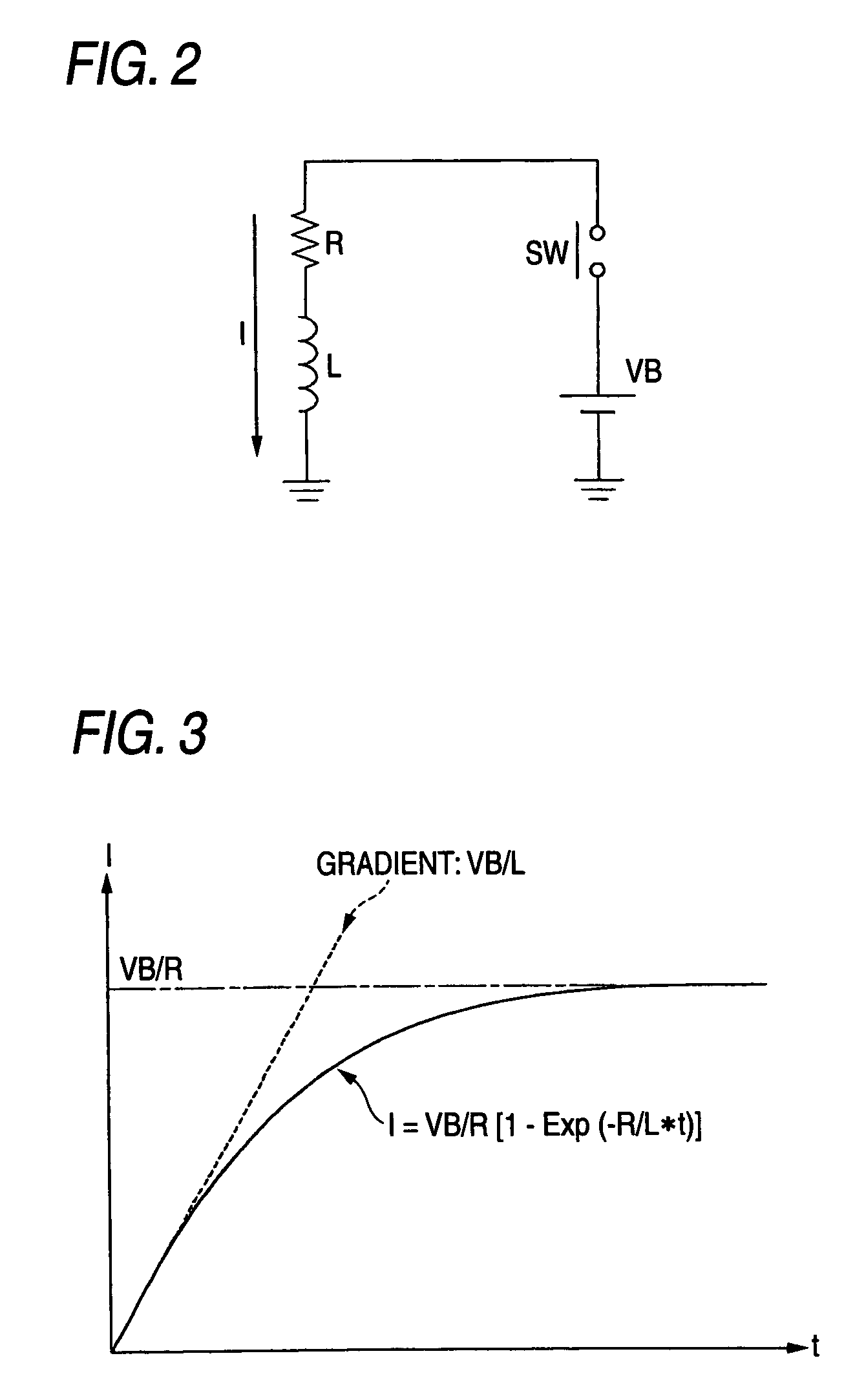
[0087]Furthermore, if the shortcircuit judging value is set to be direct proportion to the power supply voltage VB, then this shortcircuit judging value can be set to be a smaller judging value. This value setting condition will be explained in a second embodiment later.

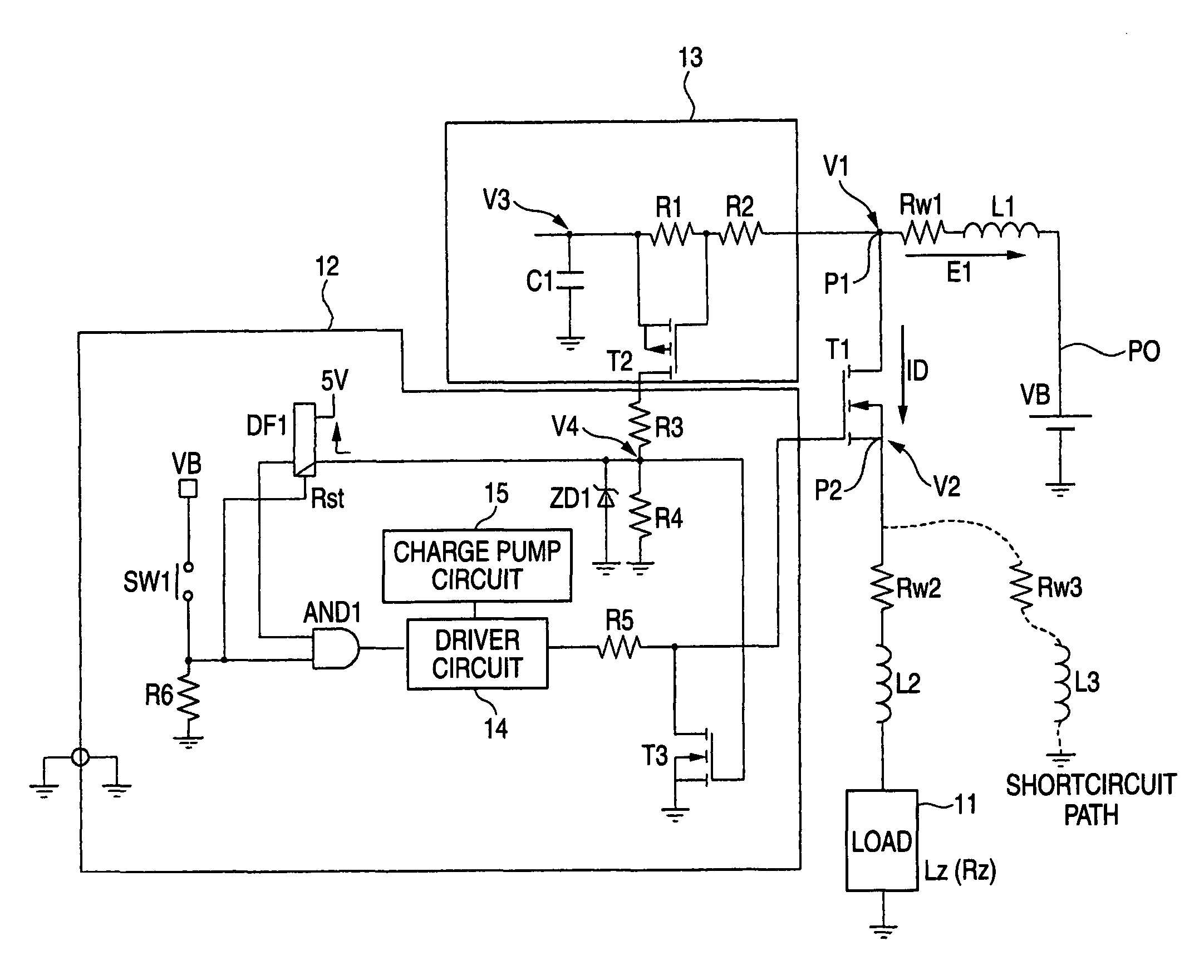
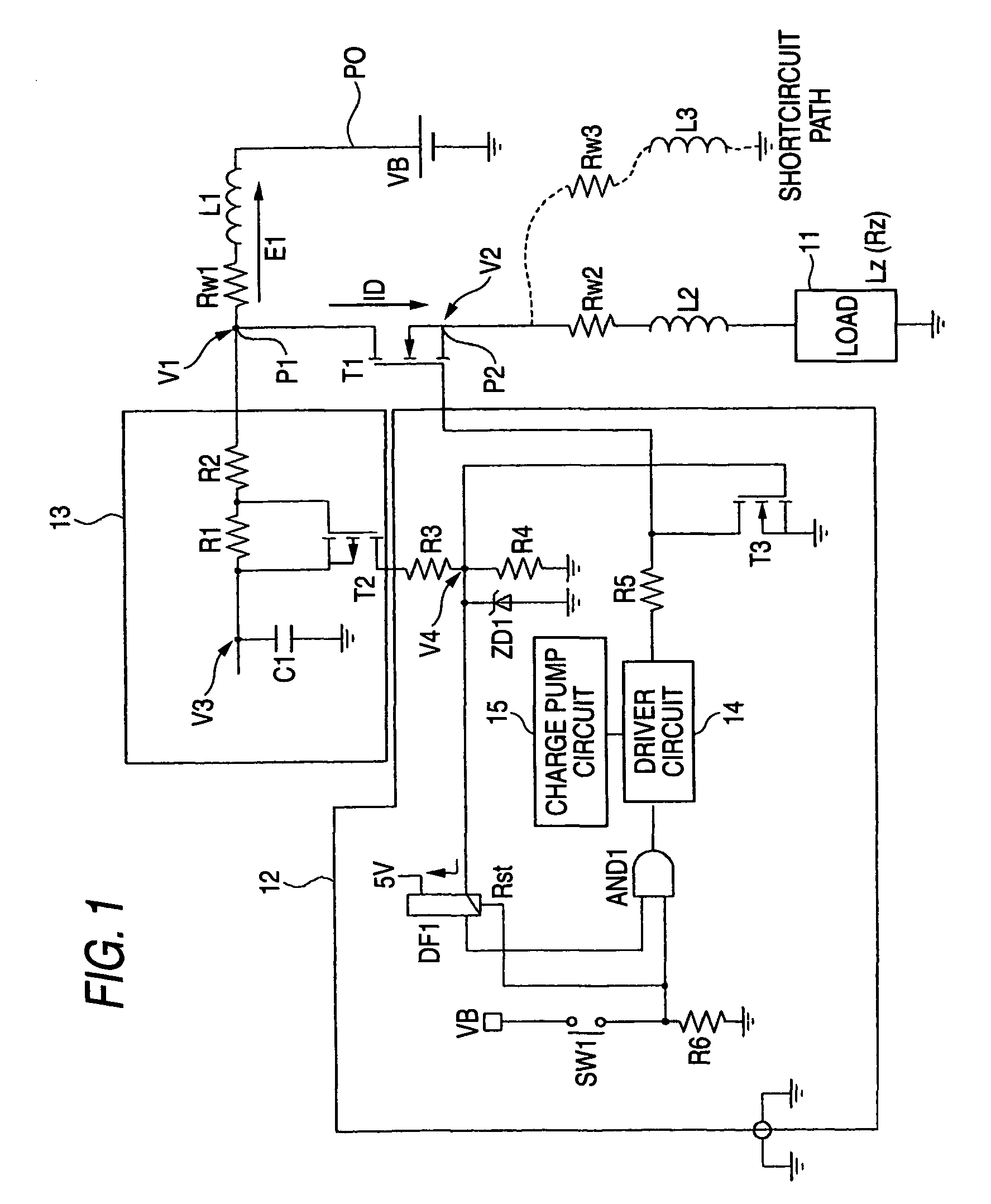
[0088]Next, a description is made of a method for detecting the counter electromotive force E1 short in the circuit shown in FIG. 1. Since such a circuit, in which the resistors R1 and R2 are series-connected to the capacitor C1, is arranged between the point P1 and the ground as the counter electromotive circuit 13, while the load 11 is operated under the normal condition, a voltage V3 at the non-grounded terminal of the capacitor C1 is charged up to the voltage V1 of the point P1. Since a voltage drop caused by that the load current ID flows through the first wiring line is small under the normal condition, the non-grounded terminal voltage V3 is nearly equal to the power supply voltage VB.

first embodiment

[0089]This voltage V3 at the non-grounded terminal of the capacitor C1 may constitute a reference voltage when the magnitude of the counter electromotive force E1 is measured. In accordance with this first embodiment, when the counter electromotive force E1 is generated and thus the voltage V1 at the point P1 is lowered, it is so judged as to whether or not a shortcircuit current flows by measuring a difference voltage between this voltage V1 and the reference voltage V3.

[0090]In other words, in such a case that the difference voltage (V3−V1) exceeds a preset threshold voltage, such a judgment is made that the short current flows in the circuit. Then, this difference voltage (V3−V1) constitutes a voltage appeared at both the terminals of the resistors R1 and R2. In this first embodiment, such a voltage across both the terminals of the resistor R1 is measured as a voltage which is partially produced in the first-mentioned voltage, so that an occurrence of such a shortcircuit current ...

third embodiment

[0130]In this third embodiment, in the case that a shortcircuit / grounding event happens to occur in any one of these plural FET channels, all of these channels are once turned OFF, and thereafter, the respective channels are sequentially and again turned ON in a constant interval so as to specify such an FET channel that the shortcircuit / grounding event occurs. This detecting operation may be carried out by a logic circuit.

[0131]FIG. 7 is a circuit diagram for indicating a sequential starting circuit for 5 channels as one example of the above-explained logic circuit. As indicated in this drawing, the sequential starting circuit includes switches SW1 to SW5, AND circuits AND11 to AND19, D type flip-flops DF11 to DF15, exclusive-NOR circuits XNOR1 to XNOR5, and also, a dock circuit CL. The switches SW1 to SW5 turn ON / OFF the MOSFETs owned by each of load circuits for 5 channels. Then, output signals SW11 to SW15 of the AND circuits AND11 to AND15 are supplied to the input terminal of ...


PUM


Abstract

A control apparatus includes a semiconductor switch that is arranged between a DC power supply and a load to control a turning ON / OFF operation of the load, a counter electromotive force judging unit that determines whether a counter electromotive force produced on a first wiring line is greater than a threshold voltage, the first wiring line connecting the semiconductor switch to the DC power supply, and a control unit that controls the semiconductor switch so as to be turned OFF when the counter electromotive force judging unit determines that the counter electromotive force is greater than the threshold voltage.

Description

BACKGROUND OF THE INVENTION[0001]The present invention is related to a control apparatus of a semiconductor switch provided between a DC power supply and a load, for turning ON / OFF the load. More specifically, the present invention is directed to a technique capable of protecting the semiconductor switch when a shortcircuit current is produced.[0002]Loads (electric appliances) such as, for instance, a motor for driving a power window, or a lamp, which are mounted on a vehicle are driven by applying a DC voltage from a battery functioning as a DC power supply to the loads. In this case, since a semiconductor switch such as a MOSFET and the like, which is provided between a load and the battery, is turned ON / OFF so that this load is controlled so as to be driven / stopped.[0003]Also, in a case that an overcurrent protecting apparatus is mounted, an overcurrent protecting apparatus immediately turns OFF the semiconductor switch for protecting both a circuit and a load when the overcurren...

Claims


Application Information

Patent Timeline
Patent Type & Authority Patents(United States)
IPC IPC(8): H02H3/08H01H47/00H03K17/04H03K17/082
CPCH03K17/0822H02H3/08H02H7/20
Inventor OHSHIMA, SHUNZOU
Owner YAZAKI CORP
Why Eureka
Try Eureka