Light emitting device, lighting equipment or liquid crystal display device using such light emitting device

a technology of light emitting device and light emitting device, which is applied in the direction of semiconductor devices, electrical devices, basic electric elements, etc., can solve the problems of led chip failure, low thermal conductivity, and poor heat radiation performance of conventional light emitting apparatus, so as to increase critical current, increase heat radiation performance, and high thermal conductivity

Active Publication Date: 2010-10-12
KK TOSHIBA +1
View PDF23 Cites 99 Cited by
  • Summary
  • Abstract
  • Description
  • Claims
  • Application Information

AI Technical Summary

Benefits of technology

[0039]According to the light emitting apparatus having the above configuration, since an aluminum nitride (AlN) co-fired substrate having a high thermal conductivity is used as a substrate (LED package) for mounting a LED chip, the apparatus can have significantly increased heat radiation performance and increased critical currents, thereby allow a large current to pass therethrough, and can have significantly increased luminance.
[0040]In addition, the reflector used in the present invention is not integrally formed with an AlN substrate body but separately formed from metal or resin material as independent parts. Thereafter, the reflector is bonded to a surface of the aluminum nitride substrate. Accordingly, the parts can be easily worked at the stage of a part, so that it becomes possible to accurately control a coarse degree of the finished surface, dimension (size), inclination angle of the light-reflecting plane or the like of the reflector with a high accuracy, whereby the reflector having an excellence in light-reflecting property can be obtained and the light-extraction efficiency can be increased.
[0041]Furthermore, the light emitting device is mounted and connected to the AlN substrate by the flip-chip method, so that the emitted light can be extracted from an entire rear surface of the light emitting device. In addition, a spacing pitch between the adjacent light emitting devices can be narrowed, so that a mounting density of the light emitting devices can be increased and the light emitting apparatus can thereby be reduced in thickness and size.

Problems solved by technology

The conventional light emitting apparatus, however, has a fatal defect of very poor heat radiation performance, since the ceramic package mounted with the LED chip comprises a ceramic material mainly composed of alumina (Al2O3) having a low thermal conductivity of about 15 to 20 W / mK, and the molding resin for sealing the LED chip also has a low thermal conductivity.
The LED chip may be broken due to heat generated upon application of a high voltage and / or a large current.
Consequently, there has been raised a problem that the conventional light emitting apparatus has a low luminance, since the highest voltage that can be applied to the LED chip is low and the current to be supplied is limited to several ten milliamperes (mA).
Further, in the above conventional light emitting apparatus, the ceramic package integrally formed with a number of concave openings for accommodating the light emitting elements is used, so that there has been posed problems such that a process of manufacturing the light emitting apparatus becomes complicate, and finished accuracy of parts constituting the apparatus is low whereby a sufficient emission property (light emitting property) cannot be obtained.
That is, a working operation for integrally forming the number of the concave openings to a hard and brittle ceramic material was an extremely difficult, so that a great working expense and processing charge were required.
On the other hand, in a case where the number of the concave openings were integrally formed to a ceramic member by drilling work at a stage of soft molded body and then the molded body was sintered, a dimension accuracy, a finishing accuracy and a dispersion of surface roughness of the concave openings were disadvantageously deteriorated due to shrinkage error and non-uniformity in material composition, whereby there was posed a problem that an aimed light-reflecting property could not be obtained.
Since this reflector is integrally formed to the ceramic substrate, a surface roughness Ra of an inner wall surface of the reflector becomes coarse to be about 0.5 μm, so that there was also posed a problem that a scattering and dispersion of the light was liable to occur.
In addition, even if a predetermined inclined angle was tried to be imparted to the inner wall of the reflector so as to control a reflecting direction of the light, a fluctuation or a dispersion of the inclined angle was large, so that it was difficult to stably impart a predetermined inclined angle.
At any rate, it was difficult to correctly control the shape accuracy of the concave openings.
Furthermore, even if a worker tried to work and adjust the reflector so as to realize a predetermined finishing accuracy, the ceramic material having hard and brittle properties was difficult to be smoothly worked, so that there was also posed a problem that a man-hour required for the working was greatly increased.
Additionally, in conventional light emitting apparatuses as shown in FIG. 2, the LED chip and the conductive interconnections are electrically connected by a wire bonding process, so that the wire and an electrode pad disposed on the LED chip partially block or intercept the emitted light, whereby there was also posed a problem that a light-extraction efficiency was decreased.
Further, a portion where the bonding wire rises protrudes in a thickness direction of the apparatus, and a large electrode region for connecting the edge of the bonding wire is disadvantageously required.
Thus, there has been posed a problem that the LED package including the interconnection structure becomes large in size.
Furthermore, when the LED chip is mounted and accommodated in a concave opening as shown in FIG. 2 so as to avoid the adverse influence of the bonding wire protruding in a thickness direction of the apparatus, the light emitted from the LED chip is absorbed by the inner wall of the concave opening to increase the light loss and thereby to decrease the luminous efficiency.
However, it is very difficult to form such a reflecting metal layer uniformly in the concave opening having a curved inner wall, and the emitted light is partially absorbed by the inner wall to invite light loss.
In addition, there has been also posed another problem that the inner wall of the concave opening itself has such a structure as to inhibit the travel or transmission of the light, and the luminance is thereby decreased.

Method used


Image

  • Light emitting device, lighting equipment or liquid crystal display device using such light emitting device
  • Light emitting device, lighting equipment or liquid crystal display device using such light emitting device

Examples


example 1

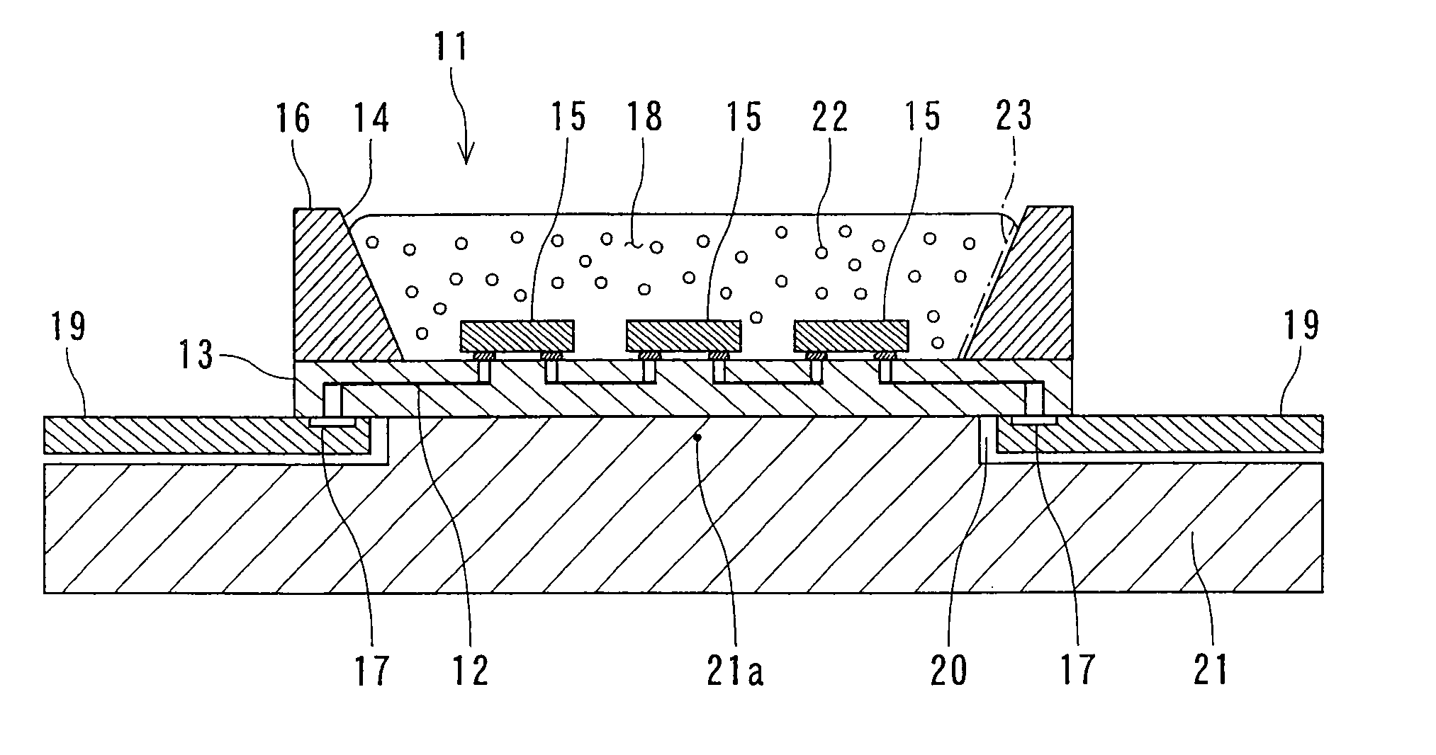
[0043]FIG. 1 is a sectional view showing an embodiment of the light emitting apparatus according to the present invention. Namely, the embodiment of the light emitting apparatus 11 is configured to comprise: an aluminum nitride co-fired substrate (AlN multi-layered substrate) 13; three LED chips 15 as light emitting devices mounted on a front surface of the co-fired AlN substrate through a flip-tip method; and a reflector 16 composed of kovar having an inclined surface 14 for reflecting a light emitted from the LED chips 15 as light emitting devices to a front side direction, the reflector 16 being solder-bonded to a surface of the aluminum nitride co-fired substrate 13 so as to surround a circumference of the LED chips 15.

[0044]As the above co-fired substrate (AlN multi-layered substrate) 13, a co-fired AlN multi-layered substrate having a high thermal conductivity of 200 W / m·K, a two-layered structure and a size of 5 mm-length×5 mm-width×0.5 mm-thickness, was used.

[0045]Further, t...

example 2

[0062]The same manufacturing process as in Example 1 was repeated except that a metal film 23 composed of silver (Ag) and having a thickness of 2 μm was formed onto the inclined surface 14 of the reflector 16 shown in FIG. 1, thereby to prepare a light emitting apparatus of Example 2.

example 3

[0063]The same manufacturing process as in Example 1 was repeated except that the heat sink 21 shown in FIG. 1 was not attached, thereby to prepare a light emitting apparatus of Example 3.


PUM


Abstract

A light emitting apparatus 11 comprises: an aluminum nitride co-fired substrate 13; at least one light emitting device 15 mounted on a front surface of the co-fired substrate 13 through a flip-tip method; and a reflector 16 having an inclined surface 14 for reflecting a light emitted from the light emitting device 15 to a front side direction, the reflector 16 is bonded to a surface of the aluminum nitride co-fired substrate 13 so as to surround a circumference of the light emitting device 15. This configuration can simplify the process of manufacturing the apparatus and can provide light emitting apparatus that are excellent in heat radiation performance, allow a larger current to pass therethrough, and can have a significantly increased luminance with a high luminous efficiency.

Description

TECHNICAL FIELD[0001]The present invention relates to a light emitting apparatus, a lighting apparatus (interior illumination) and a liquid crystal display including light emitting devices such as light emitting diodes (LEDs) or semiconductor laser arranged on surfaces of insulating substrates. More specifically, the present invention relates to a light emitting apparatus, a lighting apparatus and a liquid crystal display using the light emitting apparatus that can be manufactured through a simple process, can be reduced in size, are excellent in heat radiation performance, allow a larger current to pass therethrough, and can have a significantly increased luminance (luminescence) with a high luminous efficiency.BACKGROUND ART[0002]Light emitting diodes (hereinafter also referred to as LED chips) are light emitting devices (light emitting elements) that act as light sources upon application of a voltage and utilize light emitted as a result of recombination between electrons and pos...

Claims


Application Information

Patent Timeline
Patent Type & Authority Patents(United States)
IPC IPC(8): H01L33/00H01L33/60H01L33/64
CPCH01L33/641H01L25/0753H01L33/60H01L2224/48472H01L2224/48227H01L2924/00H01L2224/48091H01L2224/16225H01L2924/00014
Inventor YANO, KEIICHI
Owner KK TOSHIBA
Why Eureka
Try Eureka