Components and methods for use in electro-optic displays

a technology of electrooptic displays and components, applied in the direction of optics, instruments, optical elements, etc., can solve the problems of inadequate service life of these displays, unable to meet the needs of users, and gas-based electrophoretic media are susceptible to the same types of problems, so as to achieve convenient and flexible color filter arrays

Active Publication Date: 2010-11-23
E INK CORPORATION
View PDF298 Cites 726 Cited by
  • Summary
  • Abstract
  • Description
  • Claims
  • Application Information

AI Technical Summary

Problems solved by technology

Nevertheless, problems with the long-term image quality of these displays have prevented their widespread usage.
For example, particles that make up electrophoretic displays tend to settle, resulting in inadequate service-life for these displays.
Such gas-based electrophoretic media appear to be susceptible to the same types of problems due to particle settling as liquid-based electrophoretic media, when the media are used in an orientation which permits such settling, for example in a sign where the medium is disposed in a vertical plane.
Indeed, particle settling appears to be a more serious problem in gas-based electrophoretic media than in liquid-based ones, since the lower viscosity of gaseous suspending fluids as compared with liquid ones allows more rapid settling of the electrophoretic particles.
However, the methods used for assembling LCD's cannot be used with solid electro-optic displays.
This LCD assembly process cannot readily be transferred to solid electro-optic displays.
As discussed in the aforementioned U.S. Pat. No. 6,312,304, the manufacture of solid electro-optic displays also presents problems in that the optical components (the electro-optic medium) and the electronic components (in the backplane) have differing performance criteria.
Therefore, a process for manufacturing an optical component may not be ideal for manufacturing an electronic component, and vice versa.
The processing temperature can be in the range from about 300° C. to about 600° C. Subjecting many optical components to such high temperatures, however, can be harmful to the optical components by degrading the electro-optic medium chemically or by causing mechanical damage.
Electro-optic displays are often costly; for example, the cost of the color LCD found in a portable computer is typically a substantial fraction of the entire cost of the computer.
However, such equipment is costly and the areas of electro-optic media presently sold may be insufficient to justify dedicated equipment, so that it may typically be necessary to transport the coated medium from a commercial coating plant to the plant used for final assembly of electro-optic displays without damage to the relatively fragile layer of electro-optic medium.
In particular, the electrical conductivity of the lamination adhesive layer affects both the low temperature performance and the resolution of the display.
However, increasing the conductivity of the lamination adhesive layer in this manner tends to increase pixel blooming (a phenomenon whereby the area of the electro-optic layer which changes optical state in response to change of voltage at a pixel electrode is larger than the pixel electrode itself), and this blooming tends to reduce the resolution of the display.
Hence, this type of display apparently intrinsically requires a compromise between low temperature performance and display resolution, and in practice it is usually the low temperature performance which is sacrificed.
When the conductivity of the lamination adhesive layer is more than about 10 times that of the electro-optic layer, essentially the full value of the applied voltage is used to switch the electro-optic layer, so further increases in lamination adhesive conductivity do not improve electro-optic performance.
However, the lamination adhesive conductivity cannot be made too high, since then the lamination adhesive cannot maintain lateral differences in potential, with the result that resolution is lost, with at least part of the spatial information in the backplane destroyed by the lamination adhesive shorting between adjacent electrodes.

Method used


Image

  • Components and methods for use in electro-optic displays
  • Components and methods for use in electro-optic displays
  • Components and methods for use in electro-optic displays

Examples


example 1

Production of Experimental Displays

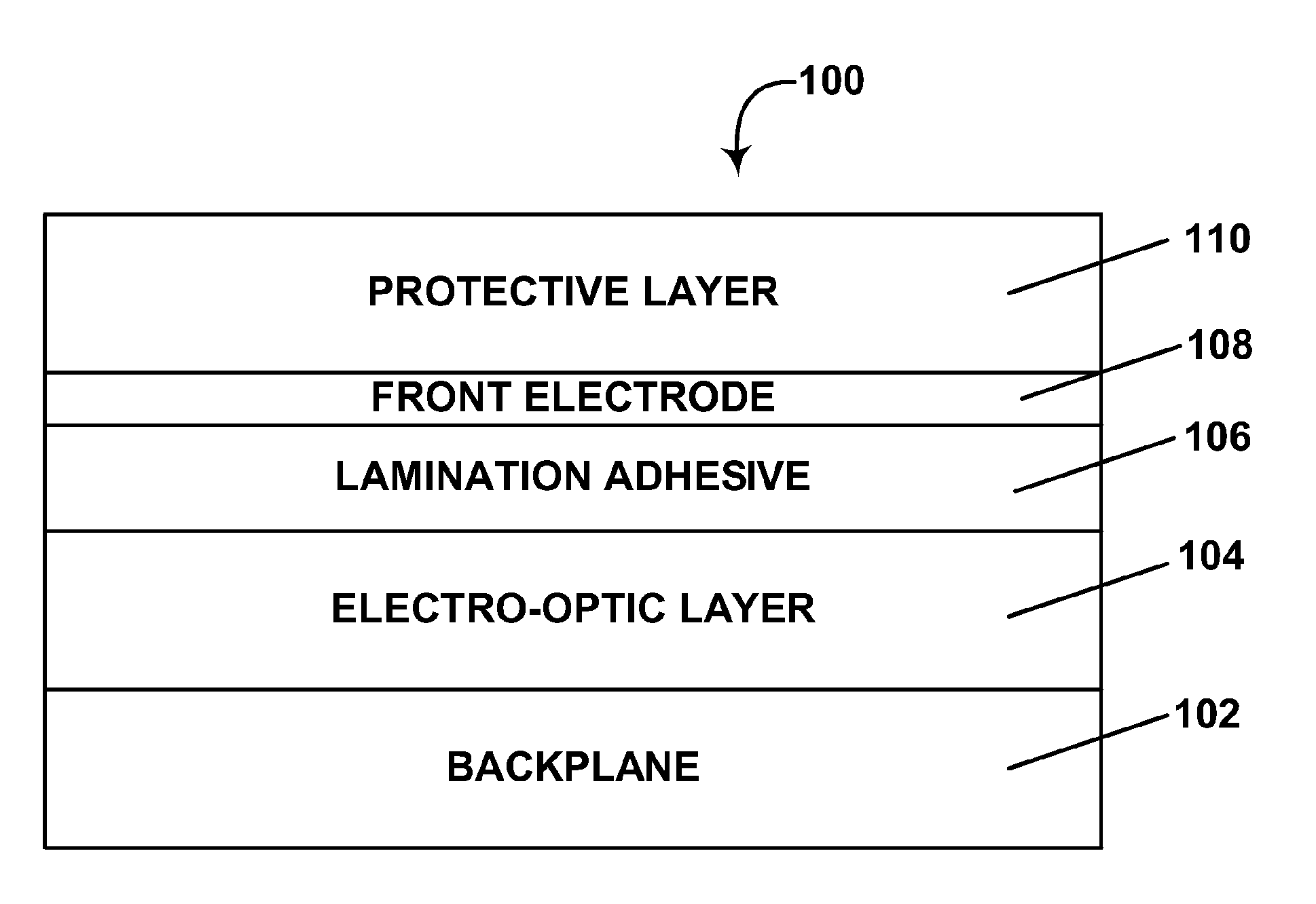
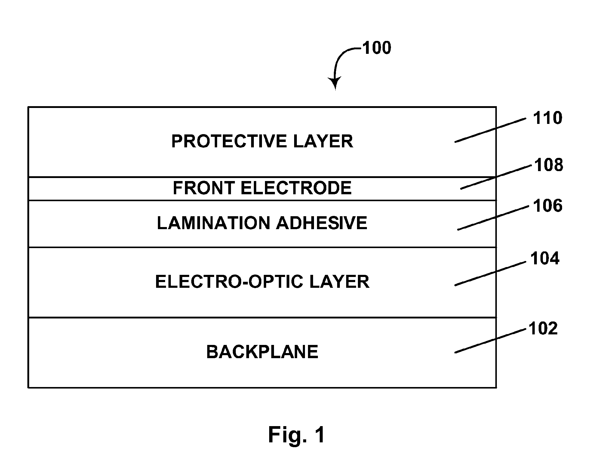
[0089]A slurry containing electrophoretic capsules in a polymeric binder was prepared substantially as described in U.S. Patent Publication No. 2002 / 0180687, Paragraphs [0067] to [0074], except that Dow Corning Q2-521 “Super Wetting Agent” was added as a coating aid. The slurry was then bar-coated on to the aluminum-coated surface of an aluminized PET release sheet. In one procedure, a 20 μm layer of a lamination adhesive had previously been coated on to the same aluminized surface; this lamination adhesive was of the type described in U.S. Pat. No. 7,012,735, and was doped with 20,000 ppm of tetrabutylammonium hexafluorophosphate. In a second procedure, the same 20 μm layer of the same lamination adhesive was laminated to the ITO-covered surface of a PET / ITO release sheet, and the resultant sub-assembly laminated to the electrophoretic layer / release sheet subassembly, the adhesive layer being laminated to the electrophoretic layer.

[0090]The lamina...

example 2

Electro-Optic Tests

[0098]The experimental displays prepared in Example 1 above were driven between their extreme black and white optical states using ±15 V, 500 millisecond drive pulses and the reflectivities of the two extreme optical states measured. Testing was effected both at room temperature (20° C.) and at 0° C. FIG. 4 of the accompanying drawings shows the dynamic range (the difference between the extreme black and white states measured in L* units (where L* has the usual CIE definition:

L*=116(R / R0)1 / 3−16,

where R is the reflectance and R0 is a standard reflectance value). In each case, the left column shows the results obtained at 20° C., while the right column shows the results obtained at 0° C.

[0099]From FIG. 4 it will be seen that the control and the “inverted” structure of the present invention (the two pairs of columns at the left-hand side of FIG. 4, the inverted layer being inverted in the sense that the electrophoretic layer is inverted) show very similar results at ...

example 3

Resolution

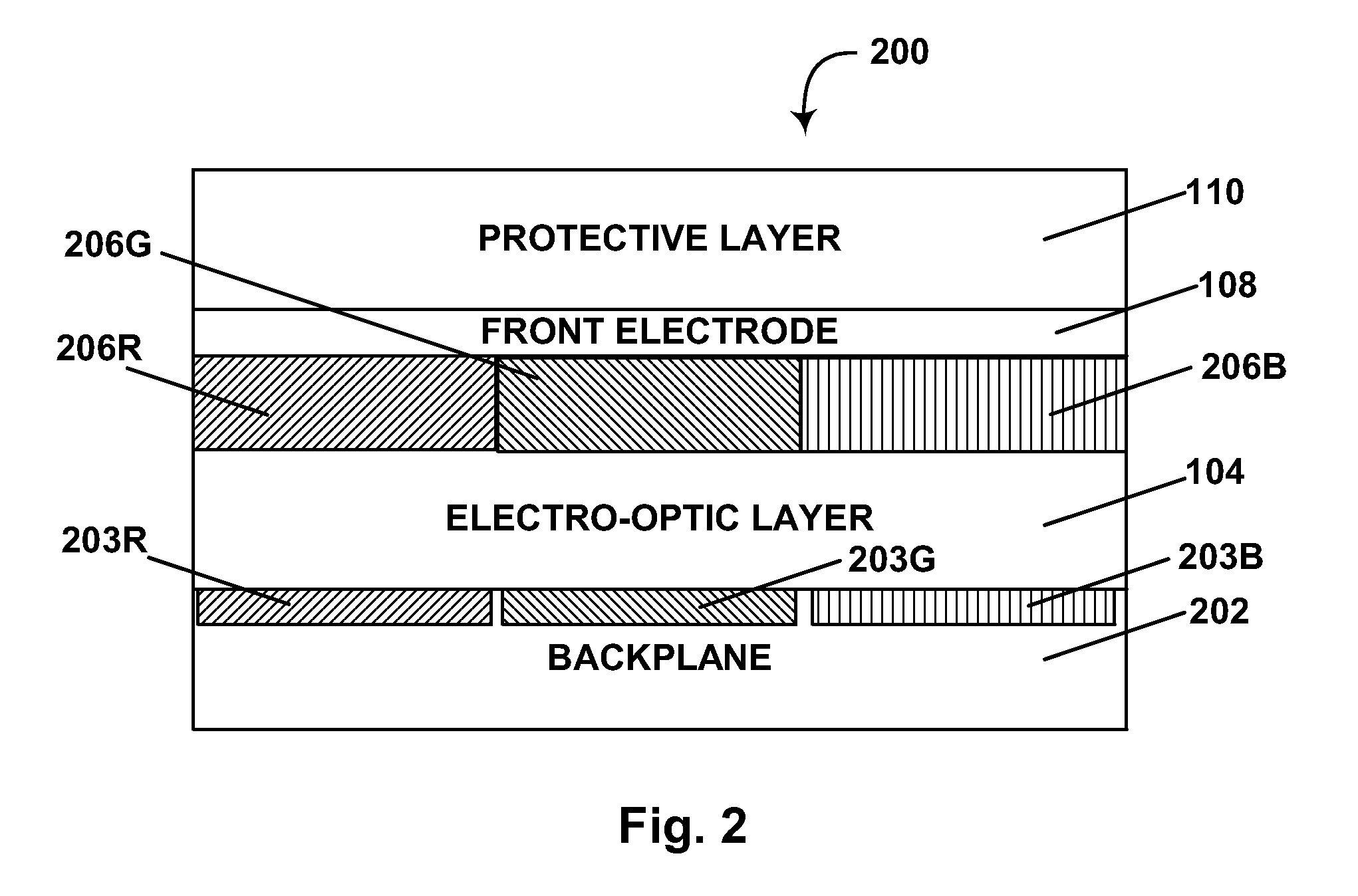
[0101]The resolution of the control displays and those of the present invention was evaluated by microscopic examination of the displays formed on glass backplanes; FIG. 5 shows the differences that were observed. As indicated in FIG. 5, each of the displays used in these tests comprised two pixels separated by a 100 μm gap having no ITO layer and hence non-switching. The control display (conventional FPL structure) is shown on the left-hand side of FIG. 5 and the display of the present invention on the right-hand side. Each side of FIG. 5 is a composite of three separate micrographs of the relevant display. The upper section of FIG. 5 shows the display with the right pixel switched to its white extreme optical state, while the lower section of FIG. 5 shows the display with the right pixel switched to its black extreme optical state.

[0102]It can be seen from FIG. 5 that, in the control display, blooming caused switching across the entire width of the inter-pixel gap, i.e.,...


PUM

PropertyMeasurementUnit
thicknessaaaaaaaaaa
particle sizeaaaaaaaaaa
temperaturesaaaaaaaaaa

Abstract

An electro-optic display comprises, in order, a backplane comprising a plurality of pixel electrodes; a layer of a solid electro-optic medium; a main adhesive layer; and at least one of a light-transmissive protective layer and a light-transmissive electrically-conductive layer. The electro-optic layer may be in direct contact with the backplane or separated therefrom by a thin auxiliary layer of adhesive. The main adhesive layer may be colored to provide a color filter array. An inverted front plane laminate useful in forming such a display comprises the same layers except that the backplane is replaced by a release sheet. The display combines good low temperature performance and good resolution at higher temperatures.

Description

REFERENCE TO RELATED APPLICATIONS[0001]This application is a continuation-in-part of application Ser. No. 10 / 605,024, filed Sep. 2, 2003 (Publication No. 2004 / 0155857), which claims benefit of application Ser. No. 60 / 319,516, filed Sep. 3, 2002.[0002]This application claims benefit of application Ser. No. 60 / 596,743, filed Oct. 18, 2005, and of application Ser. No. 60 / 596,799, filed Oct. 21, 2005.[0003]This application is related to:[0004](a) U.S. Pat. No. 6,982,178, issued Jan. 3, 2006 on application Ser. No. 10 / 249,957, filed May 22, 2003, which claims benefit of Application Ser. No. 60 / 319,300, filed Jun. 10, 2002, and Application Ser. No. 60 / 320,186, filed May 12, 2003;[0005](b) Application Ser. No. 10 / 907,065, filed Mar. 18, 2005 (Publication No. 2005 / 0146774, now U.S. Pat. No. 7,236,292), which is a divisional of the aforementioned application Ser. No. 10 / 249,957;[0006](c) U.S. Pat. No. 7,110,164, issued Sep. 19, 2006 on application Ser. No. 10 / 904,063, filed Oct. 21, 2004, wh...

Claims


Application Information

Patent Timeline
Patent Type & Authority Patents(United States)
IPC IPC(8): G02F1/29G02F1/03G02B26/00G02F1/07G02F1/167G02F1/16757
CPCG02F1/167G02F1/153G02F1/133377G02F1/1334G02F1/133514G02F2203/60G02F2001/133354G02F2202/28G02F1/16757G02F1/133354
Inventor WHITESIDES, THOMAS H.PAOLINI, JR., RICHARD J.WALLS, MICHAEL D.SOHN, SEUNGMANMCCREARY, MICHAEL D.DANNER, GUY M.HONEYMAN, CHARLES HOWIEDUTHALER, GREGG M.STEINER, MICHAEL L.RITTER, JOHN E.
Owner E INK CORPORATION
Why Eureka
Try Eureka