Semiconductor package having through holes

Active Publication Date: 2010-11-30
AMKOR TECH SINGAPORE HLDG PTE LTD
View PDF22 Cites 157 Cited by
  • Summary
  • Abstract
  • Description
  • Claims
  • Application Information

AI Technical Summary

Benefits of technology

[0009]Disclosed is a semiconductor package. The semiconductor package is configured to form a plurality of through holes for forming a through silicon via at once using a sawing device used for wafer sawing instead of a separate laser drilling equipment or a deep reactive ion etching (DRIE) equipment. Ac

Problems solved by technology

However, the laser drilling method performs laser drilling in proportion to the number of through holes and leads to long time for fabrication and high cost.
Additionally, the laser drilling method also leads to formation of a through hole in an inaccurate position, because it is difficult for the laser drilling method to accurately form the through hole in a desired position.
Side wall bowing, silicon debris or the like are caused by the laser drilling method when a through hole is formed on a wafer, resulting in generating defects of the through silicon via formed in an inner portion of

Method used


Image

  • Semiconductor package having through holes
  • Semiconductor package having through holes
  • Semiconductor package having through holes

Examples


Embodiment Construction

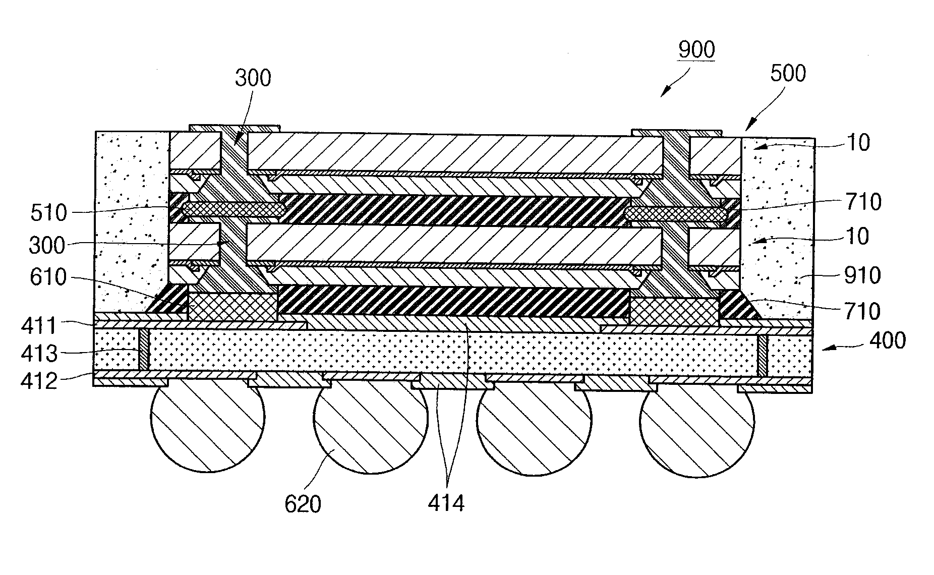
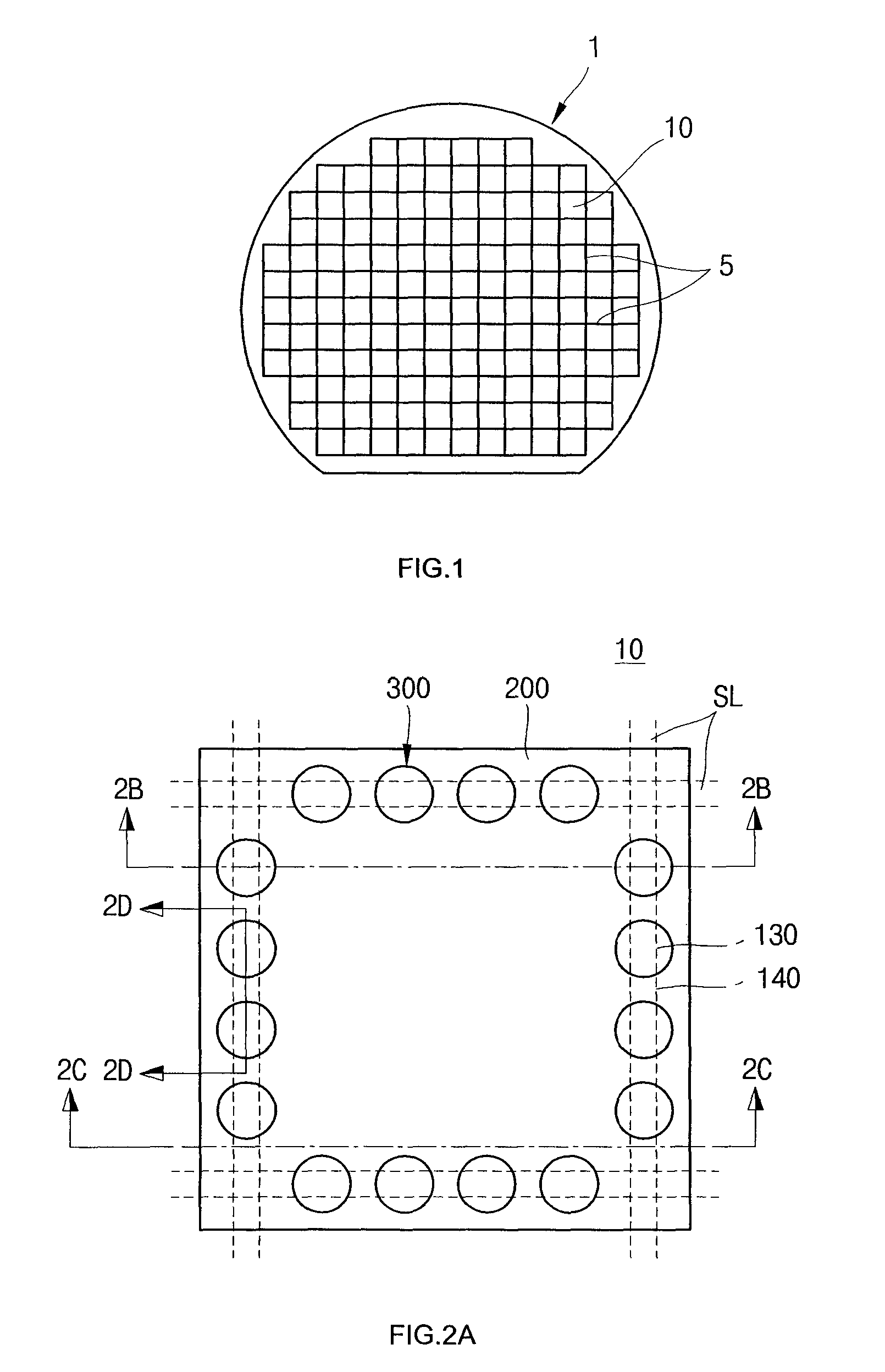
[0031]Referring to FIG. 1, a wafer on which a semiconductor package is formed according to an embodiment of the present invention is shown as a schematic plan view.

[0032]As shown in FIG. 1, a plurality of semiconductor packages 10 are formed on a wafer 1 made of a silicon material. The semiconductor packages 10 independently separated by a sawing process according to a scribing line 5 of the wafer 1 are used for various electric and electronic fields. The semiconductor packages 10 can be fabricated in a wafer level state. Hereinafter, the structure and fabricating method of one semiconductor package 10 of the semiconductor packages 10 in the wafer level state will be explained.

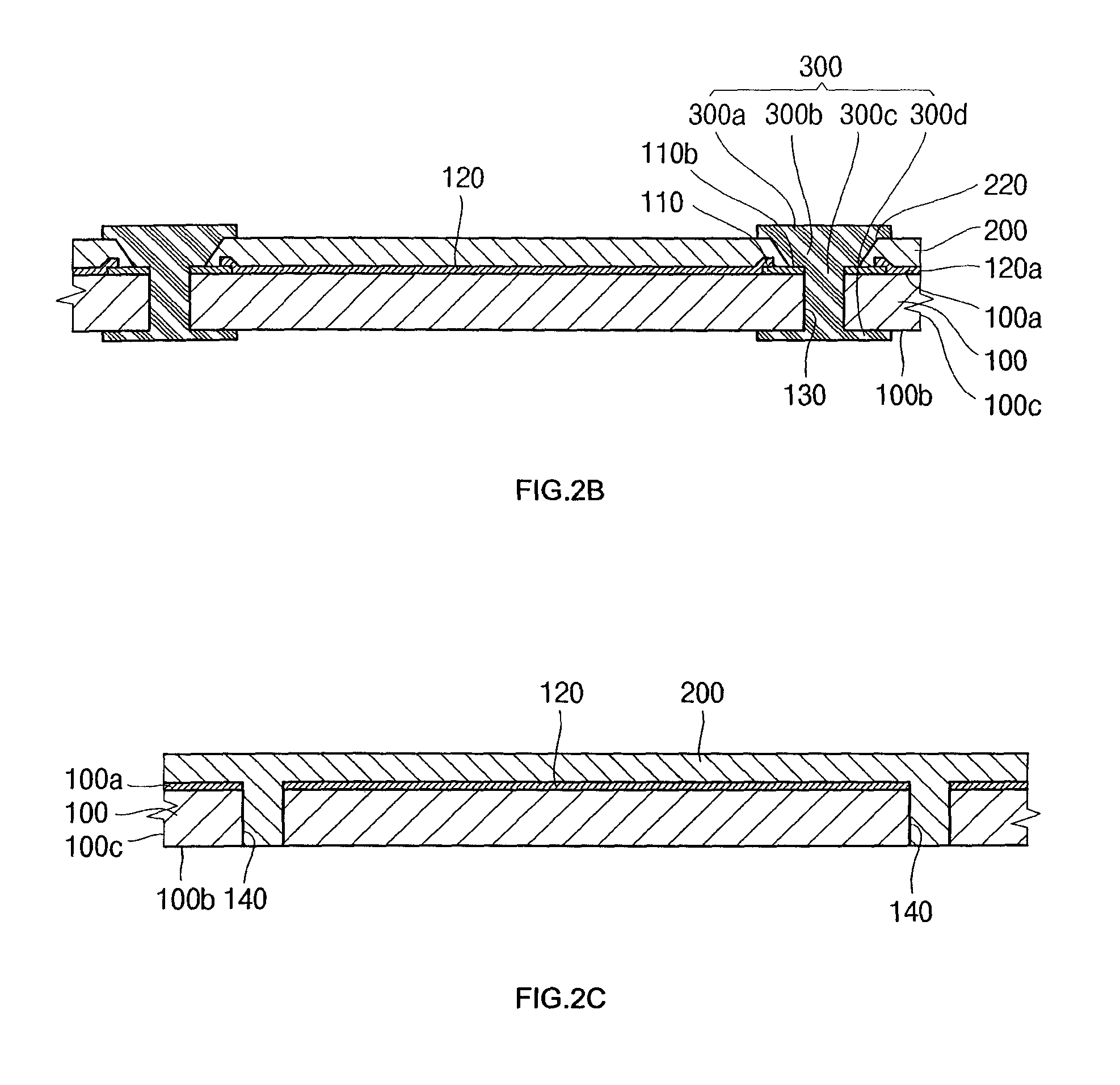
[0033]Referring to FIG. 2A, the semiconductor package 10 of FIG. 1 is shown as a plan view. Referring to FIG. 2B, a cross-sectional view is shown, taken along a 2B-2B line of FIG. 2. Referring to 2C, a cross-sectional view is shown, taken along a 2C-2C line of FIG. 2A. Referring to 2D, an enlarged cross-sectio...


PUM


Abstract

Disclosed is a semiconductor package. The semiconductor package is configured to form a plurality of through holes for forming a through silicon via at once using a sawing device used for wafer sawing instead of a separate laser drilling equipment or a deep reactive ion etching (DRIE) equipment. Accordingly, the semiconductor package saves fabricating time and increases fabrication yield, saves costs for a laser drilling equipment or a DRIE equipment, and prevents various defects generated in an inner portion of a through hole in the case of using the laser drilling equipment or the DRIE equipment.

Description

BACKGROUND OF THE INVENTION[0001]1. Field of the Invention[0002]The invention relates to a semiconductor package and a fabricating method thereof.[0003]2. Description of the Related Art[0004]Recently, portable electronic devices such as a mobile phone, a PMP and others have been required to achieve high-functionality, miniaturization, light-weight and price reduction. According to the tendency, a semiconductor package mounted in portable electronic devices has been also developed in a type of a 3D semiconductor package to be more innovative and price-competitive. The 3D-semiconductor package has been used by a semiconductor stacking technology using a through silicon via (TSV). The semiconductor stacking technology using the TSV is a technology indicating that semiconductor dies or semiconductor packages are perpendicularly stacked. The semiconductor stacking technology leads to reduction of the length between the semiconductor die and the semiconductor package, and thus achieves hi...

Claims


Application Information

Patent Timeline
IPC IPC(8): H01L23/48
CPCH01L21/76898H01L23/481H01L24/06H01L25/0657H01L25/105H01L25/50H01L21/563H01L23/3107H01L24/05H01L24/16H01L2224/0401H01L2224/05553H01L2224/05554H01L2224/05555H01L2224/06135H01L2225/06513H01L2225/06517H01L2225/06541H01L2924/01013H01L2924/01014H01L2924/01029H01L2924/0105H01L2924/01078H01L2924/01079H01L2924/01082H01L2924/014H01L2924/15311H01L2924/18161H01L2924/01033H01L2924/01047H01L2224/13025H01L2224/16145H01L2224/16225H01L2224/32145H01L2224/32225H01L2224/73204H01L2924/00H01L2225/1023H01L2225/1058
Inventor PARK, SUNG SUKIM, JIN YOUNGJIN, JEONG GI
Owner AMKOR TECH SINGAPORE HLDG PTE LTD
Why Eureka
Try Eureka