Heat dissipating semiconductor package

a technology of semiconductors and semiconductor components, applied in semiconductor devices, semiconductor/solid-state device details, electrical apparatus, etc., can solve the problems of affecting solder material can easily overflow to the substrate surface, and the heat dissipation efficiency and product reliability are affected, so as to prevent overwetting of the tim, prevent collapsing or overflow of the tim, and achieve efficient bonding

Inactive Publication Date: 2008-07-10
SILICONWARE PRECISION IND CO LTD
View PDF6 Cites 2 Cited by
  • Summary
  • Abstract
  • Description
  • Claims
  • Application Information

AI Technical Summary

Benefits of technology

[0019]Therefore, according to the present invention, inside a TIM used for connecting a heat dissipating member to a semiconductor chip, there is disposed a plurality of fillers such that when the TIM is melted by heat, the fillers can control the TIM at an appropriate height so as to prevent over-wetting of the TIM and thus prevent collapsing or overflow of the TIM caused by the over-wetting problem. Further, the fillers can support the TIM to obtain an enough thickness such that an solder bonding can be formed between the heat dissipating member and the non-active surface of the flip-chip semiconductor chip, thereby ensuring an efficient bonding between the heat dissipating member and the flip-chip semiconductor chip. Meanwhile, compared with the complicated heat dissipating structure of the prior art, the present invention simplifies the fabrication process and saves fabrication time and cost.

Problems solved by technology

However, due to high frequency operation characteristic of the high integration electronic components, much more heat is generated by the high integration electronic components during operation.
Meanwhile, the connecting area between the solder material 15 and the flip-chip semiconductor chip 12 is reduced, and even a disconnecting problem can occur, thus adversely affecting the heat dissipating efficiency and product reliability.
However, during mounting the heat dissipating member, the solder material is at a liquid state, the solder material can easily overflow to the substrate surface and accordingly causes the electricity bridge problem of the passive components on the substrate surface.
However, such a heat dissipating structure is over-complicated and its fabrication cost is high.
As a result, application of the heat dissipating structure is limited.

Method used


Image

  • Heat dissipating semiconductor package
  • Heat dissipating semiconductor package
  • Heat dissipating semiconductor package

Examples


Embodiment Construction

[0024]The following illustrative embodiments are provided to illustrate the disclosure of the present invention, these and other advantages and effects can be apparent to those skilled in the art after reading the disclosure of this specification. The present invention can also be performed or applied by other different embodiments. The details of the specification may be on the basis of different points and applications, and numerous modifications and variations can be made without departing from the spirit of the present invention.

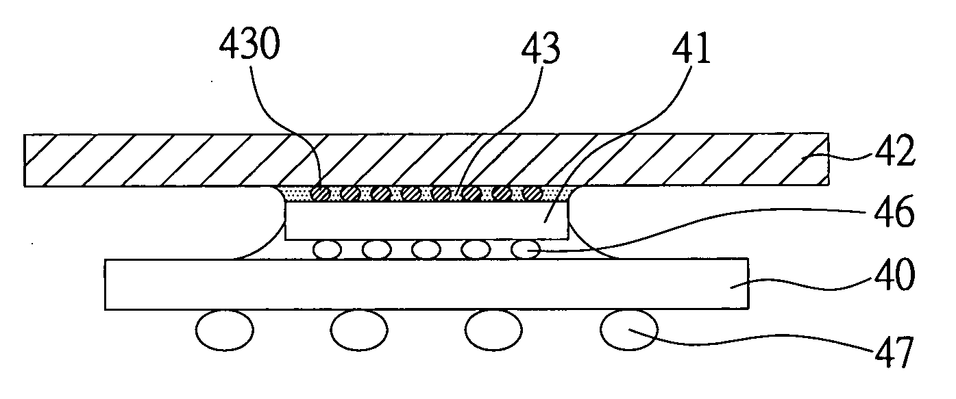
[0025]FIG. 4 is a sectional diagram of a heat dissipating semiconductor package according to the present invention.

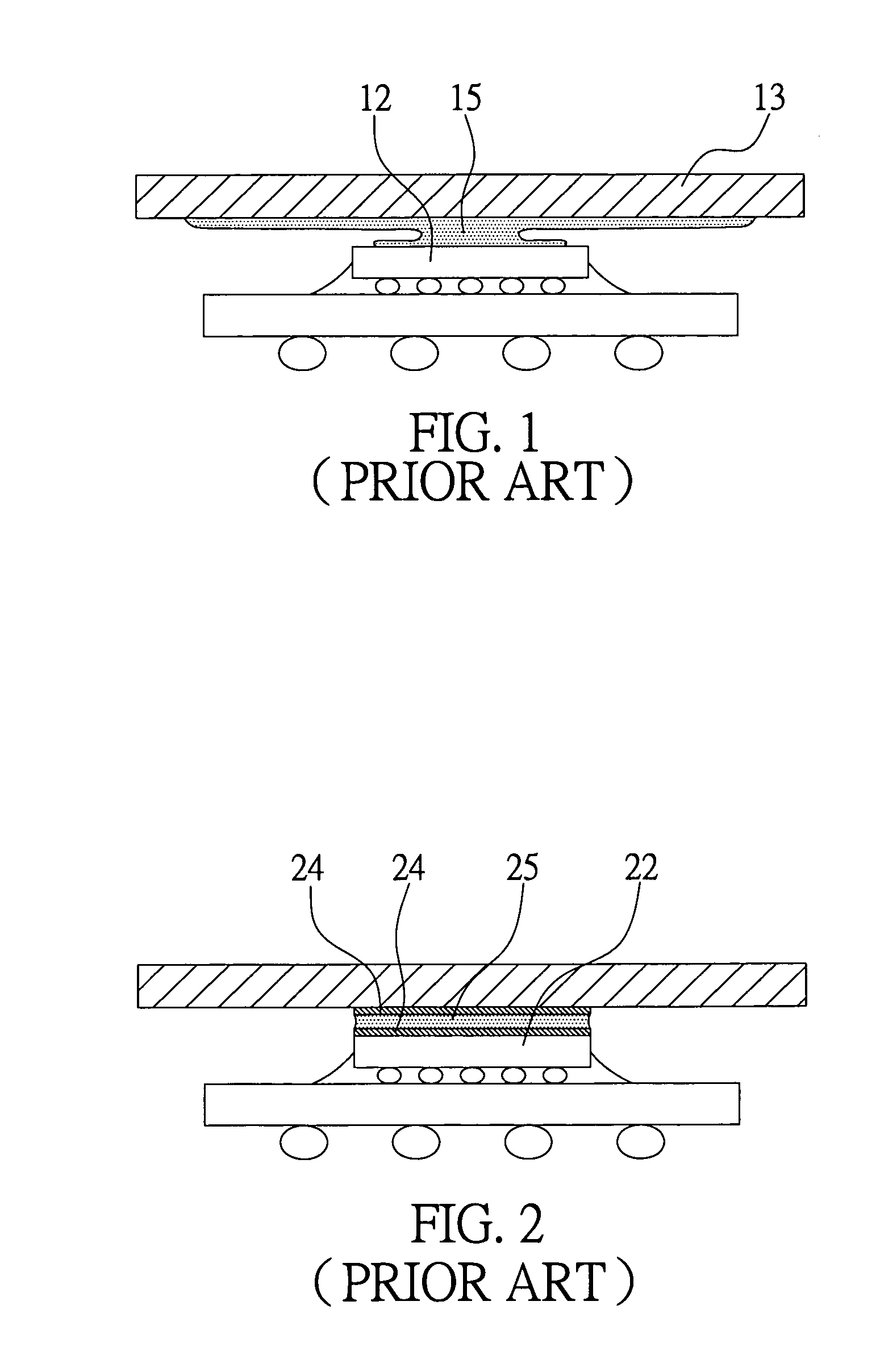
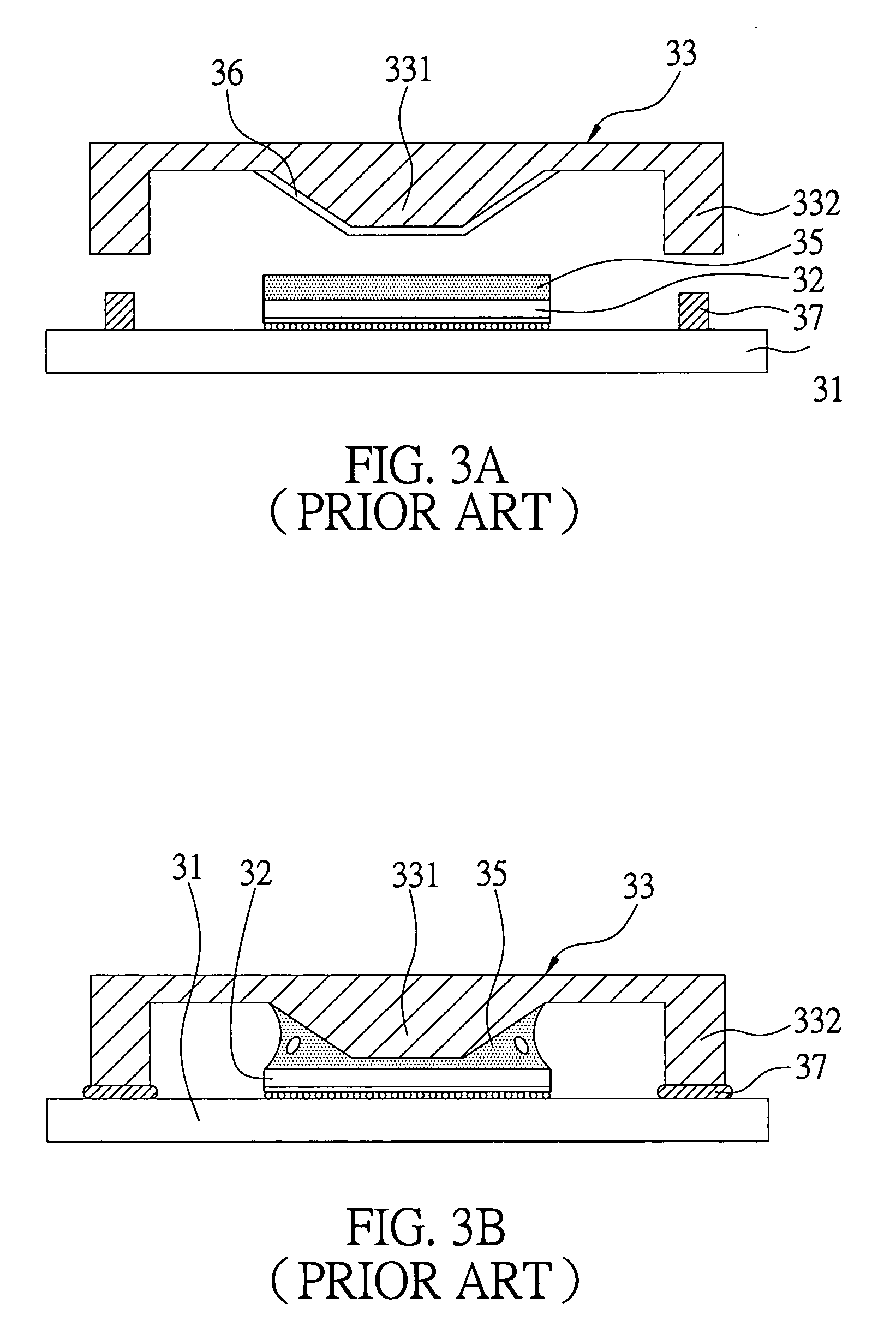
[0026]As shown in FIG. 4, the heat dissipating semiconductor package comprises: a chip carrier 40; a semiconductor chip 41 mounted and electrically connected to the chip carrier 40; and a heat dissipating member 42 mounted on the semiconductor chip 41 with a thermal interface material (TIM) 43 interposed therebetween, wherein the TIM 43 is p...


PUM


Abstract

A heat dissipating semiconductor package is disclosed, including a chip carrier; at least a semiconductor chip mounted and electrically connected to the chip carrier; and a heat dissipating member mounted on the semiconductor chip with a thermal interface material (TIM) interposed therebetween, wherein the TIM is provided with a plurality of fillers for supporting the TIM at an appropriate height, thereby preventing the TIM from being wetted so as to avoid collapsing and overflow of the TIM as a result of wetting problem.

Description

BACKGROUND OF THE INVENTION[0001]1. Field of the Invention[0002]The present invention relates generally to a semiconductor package, and more particularly to a heat dissipating semiconductor package.[0003]2. Description of Related Art[0004]In a flip chip ball grid array (FCBGA) semiconductor package, an active surface of a semiconductor chip is electrically connected with one surface of the substrate through a plurality of conductive bumps and a plurality of solder balls functioning as I / O ports is mounted to the other opposite surface of the substrate. As such a package structure greatly reduces package size, avoids conventional bonding wire design, reduces resistance, improves electrical performance and prevents signal fading in signal transmission process, it has become a mainstream package technique for next generation chips and electronic components and is particularly applied in high integration electronic components so as to meet size and operation requirements thereof. Howeve...

Claims


Application Information

Patent Timeline
Patent Type & Authority Applications(United States)
IPC IPC(8): H01L23/34
CPCH01L23/3675H01L23/42H01L2224/16H01L2224/73253H01L2924/01019H01L2924/15311H01L2924/16152H01L2924/01079H01L2924/00014H01L2924/00011
Inventor HUNG, LIANG-YIWANG, YU-POHSIAO, CHENG-HSU
Owner SILICONWARE PRECISION IND CO LTD
Why Eureka
Try Eureka