Semiconductor device and fabrication method thereof

a technology of semiconductor devices and fabrication methods, applied in semiconductor devices, semiconductor/solid-state device details, electrical apparatus, etc., can solve the problems of low-k dielectric layer having a high coefficient of thermal expansion (cte), low elastic modulus, and general brittleness, so as to avoid the generation of high thermal stress, avoid circuit or interface delamination or cracking, and reduce fabrication costs

Active Publication Date: 2012-09-06
SILICONWARE PRECISION IND CO LTD
View PDF37 Cites 0 Cited by
  • Summary
  • Abstract
  • Description
  • Claims
  • Application Information

AI Technical Summary

Benefits of technology

[0027]Since the low-k dielectric layer of the semiconductor device of the present invention is disposed far from the flip-chip mounting surface of the semiconductor structure, the present invention avoids the generation of high thermal stress during the flip-chip process due to mismatch of the coefficients of thermal expansion of the low-k dielectric layer and an adjacent material, thereby avoiding circuit or interface delamination or cracking. Further, the buffer layer covering the low-k dielectric layer can protect the low-k dielectric layer against damage caused by external influences. Furthermore, the semiconductor structure eliminates the need of a carrier board as in the prior art, thereby reducing the fabrication cost. In addition, the present invention allows the fabrication processes to be performed at the wafer level so as to save fabrication time and cost.

Problems solved by technology

Further, along with the miniaturization of electronic products, the minimum line width and pitch in a wafer process can reach 40 nm and even 28 nm However, electromagnetic noise or inductive effects can easily occur in a fine-pitch semiconductor chip, thus adversely affecting the electrical performance of the semiconductor chip.
However, the low-k dielectric layer has a high coefficient of thermal expansion (CTE) and a low elastic modulus and is generally brittle.
Furthermore, due to a large difference between the coefficients of thermal expansion of the low-k dielectric layer and the chip material, high thermal stress can occur under heat, which can easily cause circuit or interface delamination or cracking.
However, the proposed solution requires an additional carrier board such that the chip can be disposed in a cavity of the carrier board, thereby greatly increasing the overall fabrication cost and time.

Method used


Image

  • Semiconductor device and fabrication method thereof
  • Semiconductor device and fabrication method thereof
  • Semiconductor device and fabrication method thereof

Examples


Embodiment Construction

[0029]The following illustrative embodiments are provided to illustrate the disclosure of the present invention and its advantages, these and other advantages and effects being apparent to those in the art after reading this specification.

[0030]It should be noted that the drawings are not intended to limit the present invention. Various modifications and variations can be made without departing from the spirit of the present invention. Further, terms such as “one”, “above”, etc. are merely for illustrative purposes and should not be construed to limit the scope of the present invention.

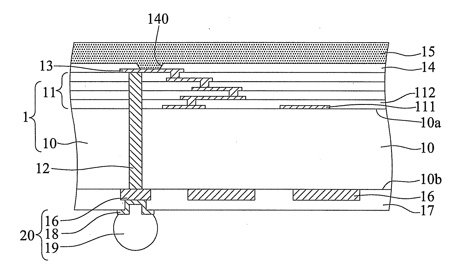
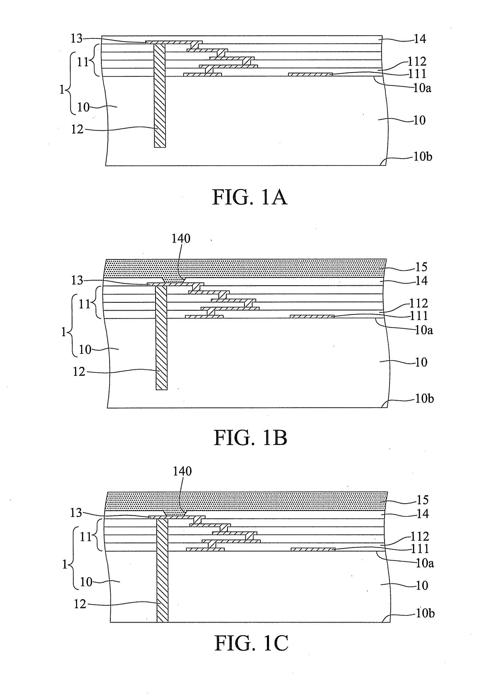
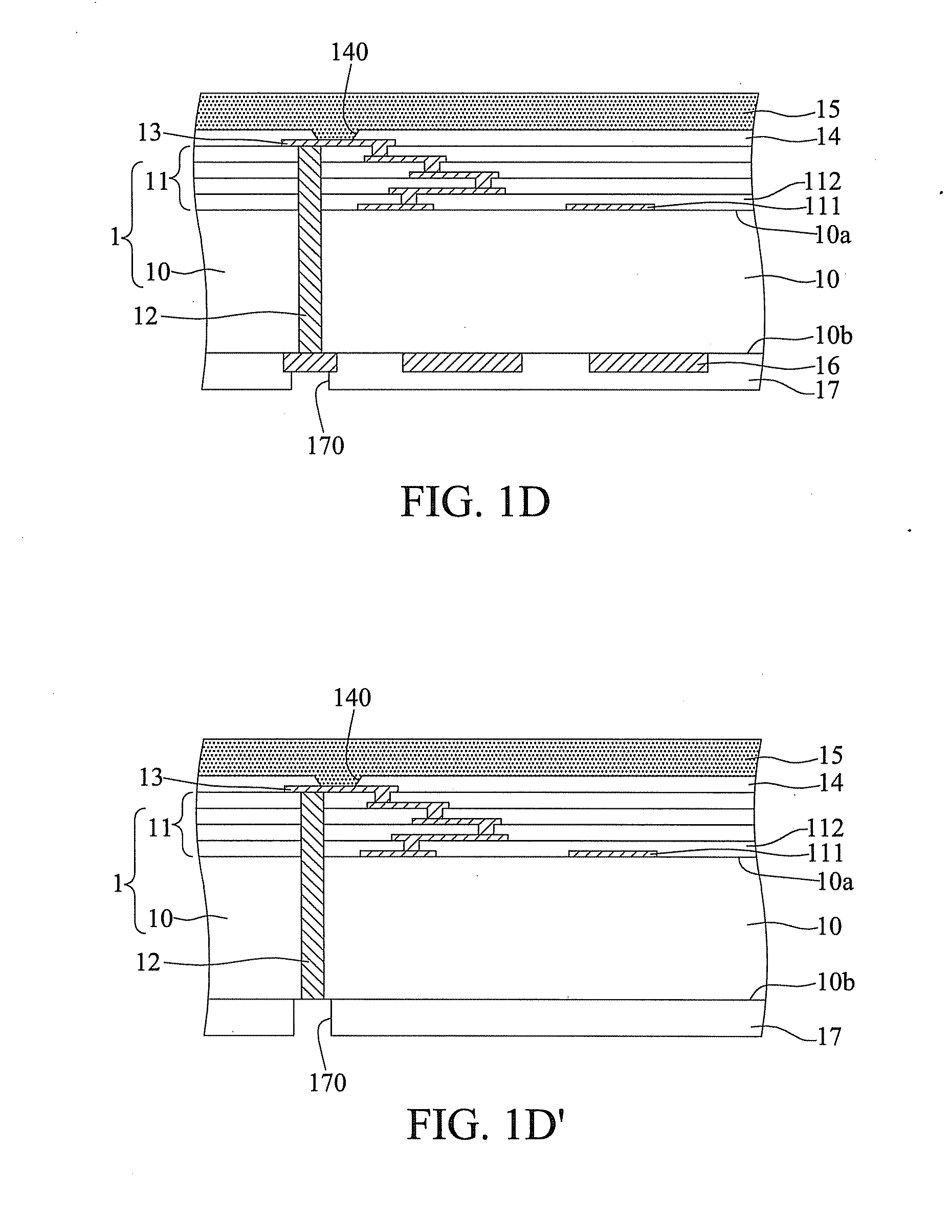
[0031]FIGS. 1A to 1F are cross-sectional views showing a semiconductor device and a fabrication method thereof according to the present invention, wherein 1D′ and 1F′ show other embodiments of 1D and 1F, respectively.

[0032]Referring to FIG. 1A, a chip 1 is provided, which has a silicon-based layer 10 having opposite first and second surfaces 10a, 10b, and a build-up structure 11 formed on the first su...


PUM


Abstract

A semiconductor structure includes a chip, a plurality of metal posts disposed in the chip and a buffer layer disposed on the chip. The chip includes a silicon-based layer having opposite first and second surfaces, and a build-up structure formed on the first surface of the silicon-based layer consisting of at least a metal layer and a low-k dielectric layer alternatively stacked on one another. Each of the metal posts is disposed in the silicon-based layer with one end thereof electrically connected with the metal layer while the other end is exposed from the second surface of the silicon-based layer. The buffer layer is disposed on the build-up structure. By positioning the low-k dielectric layer far from the second surface that is used for connecting to an external electronic component, the present invention reduces the overall thermal stress.

Description

BACKGROUND OF THE INVENTION[0001]1. Field of the Invention[0002]The present invention relates to semiconductor devices and fabrication methods thereof, and, more particularly, to a semiconductor device having a low-k dielectric layer and a fabrication method thereof.[0003]2. Description of Related Art[0004]Generally, flip-chip mounting involves electrically connecting an active surface of a chip (or other semiconductor structures) to one surface of a substrate through a plurality of metal bumps, and mounting a plurality of solder balls serving as I / O connections on the other surface of the substrate, as disclosed in U.S. Pat. No. 6,008,534, U.S. Pat. No. 6,225,704, and U.S. Pat. No. 6,372,544. The flip-chip mounting technology leads to a reduced size of the overall package structure, and also eliminates the need of bonding wires, thereby reducing the resistance, improving the electrical performance and avoiding signal distortions during transmission. Therefore, flip-chip mounting te...

Claims


Application Information

Patent Timeline
Patent Type & Authority Applications(United States)
IPC IPC(8): H01L23/498H01L21/768
CPCH01L23/481H01L2924/00014H01L2224/02372H01L24/05H01L24/13H01L2224/05548H01L2224/0557H01L2224/13022H01L2224/131H01L2224/05572H01L23/522H01L2224/0401H01L2224/05552
Inventor HUANG, HUI-MINLIN, CHUN-TANGLEE, CHIEN-WEIWANG, YEN-PING
Owner SILICONWARE PRECISION IND CO LTD
Why Eureka
Try Eureka