Package having MEMS element and fabrication method thereof

a technology of microelectromechanical system and packaging, which is applied in the direction of semiconductor devices, semiconductor/solid-state device details, electrical apparatus, etc., can solve the problems of reducing the reliability of electrical connection between the chip, affecting the miniaturization of the package structure, and poor electrical connection, so as to reduce the overall thickness of the package, simplify the fabrication process, and increase the package thickness

Inactive Publication Date: 2012-11-15
SILICONWARE PRECISION IND CO LTD
View PDF31 Cites 7 Cited by
  • Summary
  • Abstract
  • Description
  • Claims
  • Application Information

AI Technical Summary

Benefits of technology

[0017]Through the step of removing the carrier, the present invention obtains a carrier-free package. Compared with the conventional art that requires a substrate or lead frame that increases the package thickness, the present invention reduces the overall thickness of the package so as to achieve miniaturization. Further, by forming the conductors in the protection layer, the present invention avoids a conventional drilling process so as to simplify the fabrication process and reduce the fabrication cost.
[0018]Furthermore, since the package can be fabricated through wafer-level packaging without the need of a conventional substrate or lead frame, a lot of fabrication steps can be avoided so as to save fabrication time and reduce costs.

Problems solved by technology

However, the carriers of the above-described structures (the substrate 10 of FIG. 1A and the lead frame 10′ of FIG. 1B) increase the thickness of the structures, thus adversely affecting miniaturization of the package structures.
Further, it is difficult to align the conductive pads 122 at the two ends of each of the conductive through holes 120 with a high degree of accuracy or stably secure the conductive pads 122 to the conductive through holes 120, thus easily leading to poor electrical connection and accordingly reducing the reliability of electrical connection between the chip 14 and an external electronic component.

Method used


Image

  • Package having MEMS element and fabrication method thereof
  • Package having MEMS element and fabrication method thereof
  • Package having MEMS element and fabrication method thereof

Examples


Embodiment Construction

[0021]The following illustrative embodiments are provided to illustrate the disclosure of the present invention and its advantages, these and other advantages and effects being apparent to those in the art after reading this specification.

[0022]It should be noted that the drawings are only for illustrative purposes and not intended to limit the present invention. Meanwhile, indicators such as ‘up’, ‘down’, ‘a’ and so on are only used as a matter of descriptive convenience and not intended to have any other significance or provide limitations for the present invention.

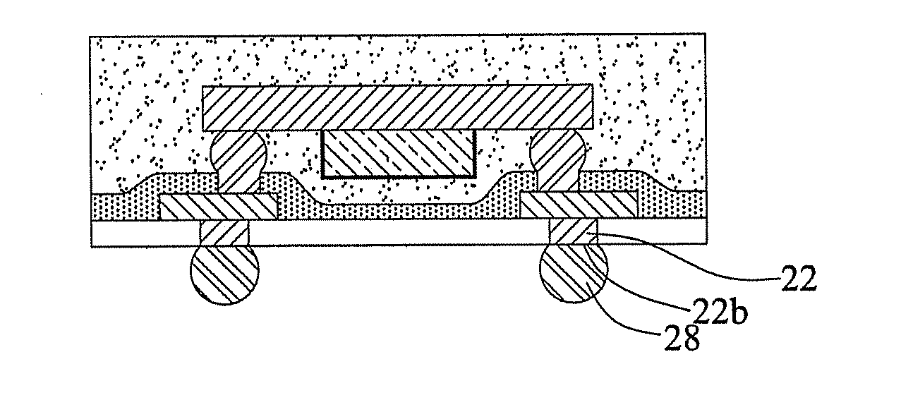
[0023]FIGS. 2A to 2I show a fabrication method of a package having a MEMS element according to the present invention.

[0024]Referring to FIG. 2A, a carrier 20 is provided. A protection layer 21 having a first surface 21a and a second surface 21b, is formed on the carrier 20 with the second surface 21b attached to the carrier 20. In the present embodiment, the carrier 20 is a metal plate, and the protection layer 21 is ma...


PUM


Abstract

A package structure having an MEMS element is provided, which includes: a protection layer having openings formed therein; conductors formed in the openings, respectively; conductive pads formed on the protection layer and the conductors; a MEMS chip disposed on the conductive pads; and an encapsulant formed on the protection layer for encapsulating the MEMS chip. By disposing the MEMS chip directly on the protection layer to dispense with the need for a carrier, such as a wafer or a circuit board that would undesirably add to the thickness, the present invention reduces the overall thickness of the package to thereby achieve miniaturization.

Description

BACKGROUND OF THE INVENTION[0001]1. Field of the Invention[0002]The present invention relates to semiconductor packages, and, more particularly, to a semiconductor package having a MEMS (micro-electro-mechanical system) element.[0003]2. Description of Related Art[0004]MEMS elements have integrated electrical and mechanical functions and can be fabricated through various micro-fabrication technologies. A MEMS element can be disposed on a chip and covered by a shield or packaged with an underfill adhesive so as to form a MEMS package structure. FIGS. 1A to 1D show various types of MEMS package structures in the art.[0005]FIG. 1A shows a MEMS package structure as disclosed by U.S. Pat. No. 6,809,412. Referring to FIG. 1A, a chip 14 having a MEMS element 141 is disposed on a substrate 10 and electrically connected to the substrate 10 through a plurality of bonding wires 11. Then, a glass lid 12 is disposed on the substrate 10 to cover the chip 14, the MEMS element 141 and the bonding wi...

Claims


Application Information

Patent Timeline
Patent Type & Authority Applications(United States)
IPC IPC(8): H01L23/498H01L21/56
CPCB81C1/00301B81B2207/096H01L2224/16225H01L2224/48091H01L2924/1461H01L2224/48465H01L2224/48227H01L2924/00014H01L2924/00H01L2924/15311H01L2924/181H01L2924/00012
Inventor CHAN, CHANG-YUEHHUANG, CHIEN-PINGKE, CHUN-CHICHIU, SHIH-KUANG
Owner SILICONWARE PRECISION IND CO LTD
Why Eureka
Try Eureka