Frequency synthesizer circuitry employing delay line
- Summary
- Abstract
- Description
- Claims
- Application Information
AI Technical Summary
Benefits of technology
Problems solved by technology
Method used
Image
Examples
Embodiment Construction
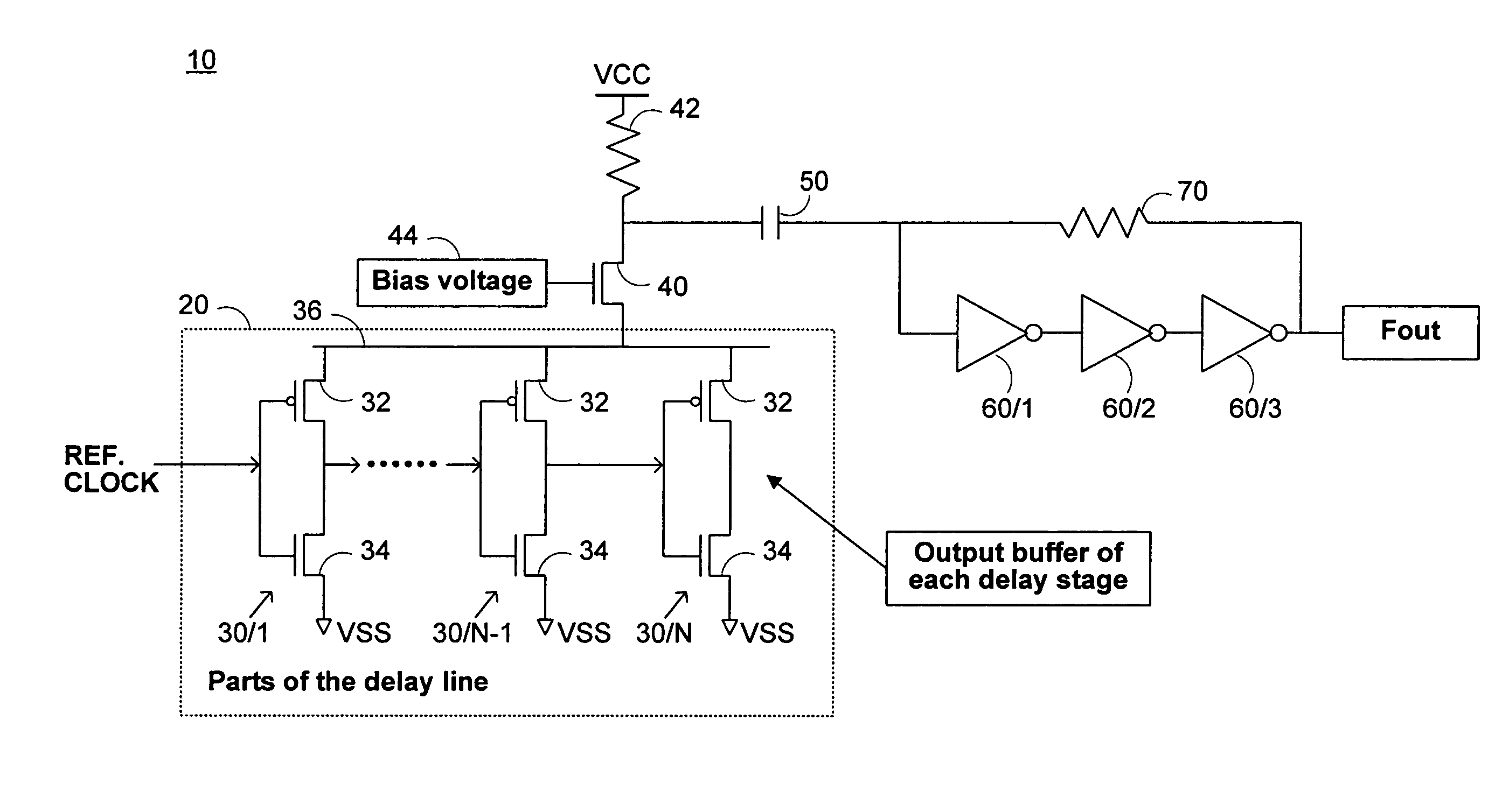
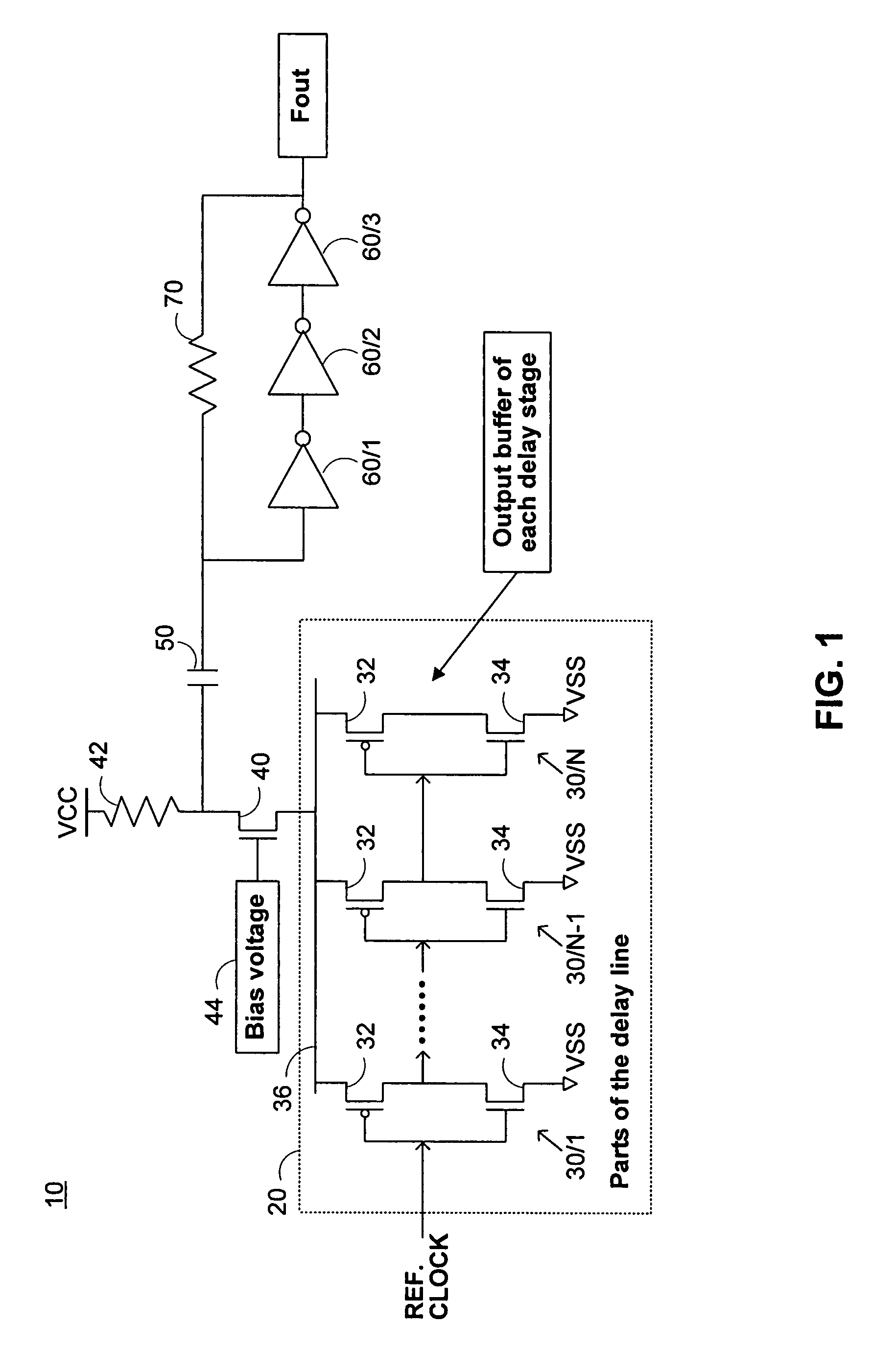
[0008]Illustrative frequency synthesizer circuitry 10 in accordance with the invention is shown in FIG. 1. Circuitry 10 includes a delay line 20, of which representative parts are shown. In particular, FIG. 1 shows the output buffers 30 / 1, 30 / N−1, and 30 / N of several representative stages of delay line 20. For example, delay line 20 may include 64 stages or any other desired number of stages. Each output buffer 30 includes a PMOS transistor 32 connected in series with an NMOS transistor 34 between a current-adding rail or node 36 and ground (VSS). Current-adding node 36 is common to all of output buffers 30. The current drawn by all of output buffers 30 is therefore added by or on rail 36.
[0009]A reference clock signal propagates through delay line 20. Each stage of the delay line inverts and delays that signal by a small amount before applying it to the next successive stage. (Although FIG. 1 only shows the output buffer 32 / 34 of each delay line stage, it will be understood that ea...
PUM
 Abstract
Description
Claims
Application Information

