Analog-to-digital converter and communication device and wireless transmitter and receiver using the same

a technology of analog-to-digital converter and communication device, which is applied in the direction of code conversion, transmission systems, instruments, etc., can solve the problems of increasing power consumption and achieve the effect of reducing the circuit area

Inactive Publication Date: 2010-11-30
HITACHI LTD
View PDF12 Cites 7 Cited by
  • Summary
  • Abstract
  • Description
  • Claims
  • Application Information

AI Technical Summary

Benefits of technology

[0014]Recently, a demand for a broadband radio device has rapidly increased including the data rate of a wireless LAN or a mobile phone. In particular, if the data rate exceeds about 100 Mbps, sample rate of several hundreds MS / s is needed. Also, in order to maintain interference wave resistance, high resolution of 10 bits or more is needed. A need exists for mounting on a radio device a calibration type analog-to-digital converter that can realize high-speed high-resolution analog-to-digital conversion while having low power consumption.
[0015]In order to realize the high sample rate and high-resolution conversion with low power consumption, the calibration type analog-to-digital converter is recently gained interest. In particular, the reason the calibration type analog-to-digital converter, which is concomitantly used with the reference analog digital conversion unit, has gained interest is because it has a short convergence time and can realize the digital calibration of a simple algorithm, as described in the Yun Chiu and the Takashi Ohshima.
[0016]The background calibration type analog-to-digital converter performs the calibration by using signals input from the antenna. In other words, the background calibration type analog-to-digital converter performs the calibration by using the signals received by the radio device without generating signals for self calibration. If the background type calibration method is used, there is an advantage that the calibration type analog-to-digital converter, which is necessary for the high-data rate radio device, can continuously performs bi-directional communication depending on a frequency division duplex (FDD) method that divides a channel according to a use frequency.
[0017]However, the background calibration type analog-to-digital converter generally occupies a large area because of the phase compensating capacity of the op-amp included in the reference analog-to-digital conversion unit. In addition, the calibration type analog-to-digital converter generally includes the sample and holds circuit to exclude the influence of parasitic capacitance of wirings, thereby increasing power consumption.
[0020]The main problem to be solved by the present invention is to provide an analog-to-digital converter and a communication device and a wireless transmitter and receiver circuit using the same, which can perform high-speed and high precision digital calibration necessary for a high-data rate communication device without increasing a circuit area.
[0022]According to the present invention, the reference analog-to-digital conversion unit among the calibration type analog-to-digital converters, which is necessary for the high-data rate communication device, is substituted into the digital-to-analog converter for transmission, thereby decreasing the circuit area.

Problems solved by technology

In addition, the calibration type analog-to-digital converter generally includes the sample and holds circuit to exclude the influence of parasitic capacitance of wirings, thereby increasing power consumption.

Method used


Image

  • Analog-to-digital converter and communication device and wireless transmitter and receiver using the same
  • Analog-to-digital converter and communication device and wireless transmitter and receiver using the same
  • Analog-to-digital converter and communication device and wireless transmitter and receiver using the same

Examples


first embodiment

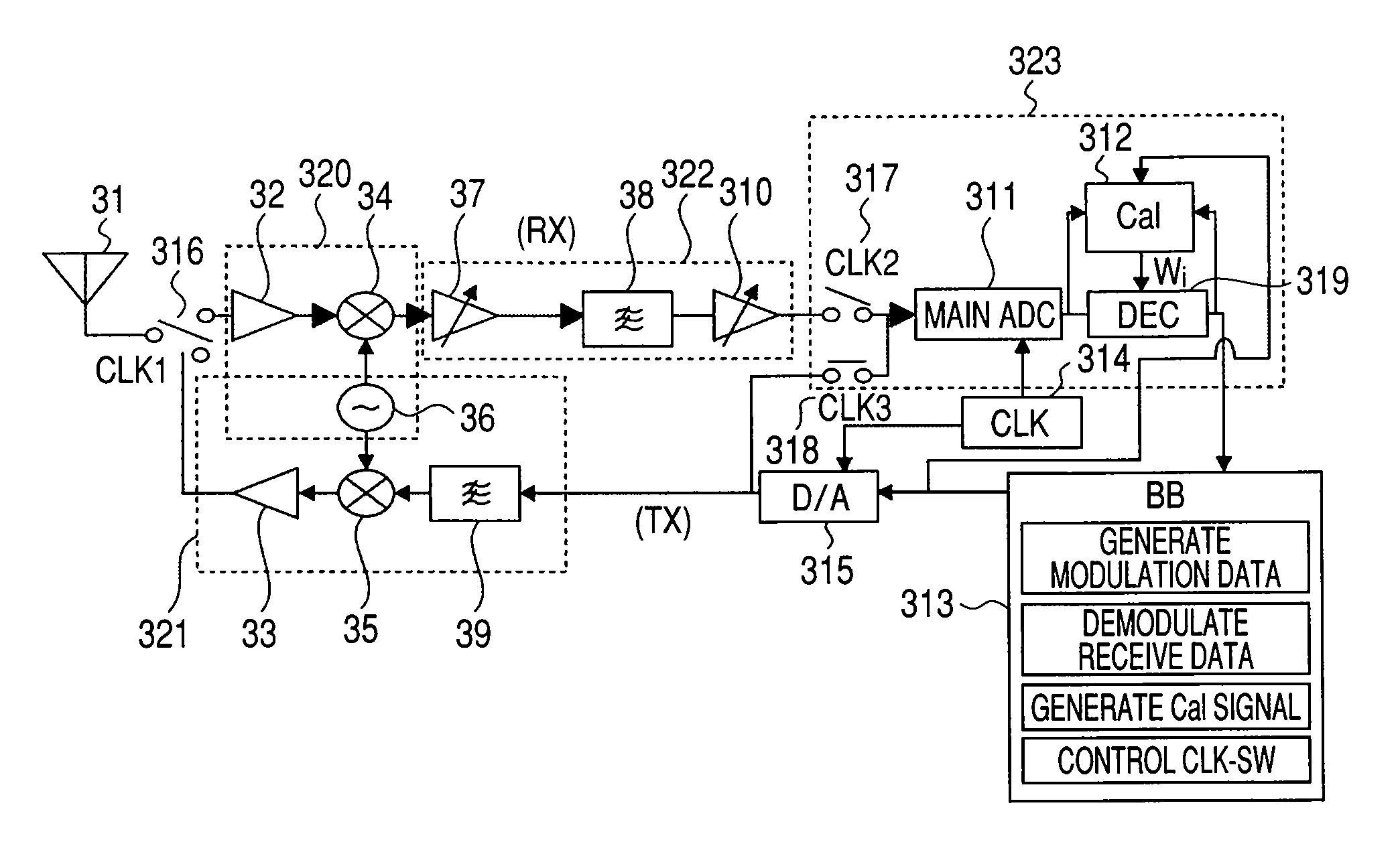
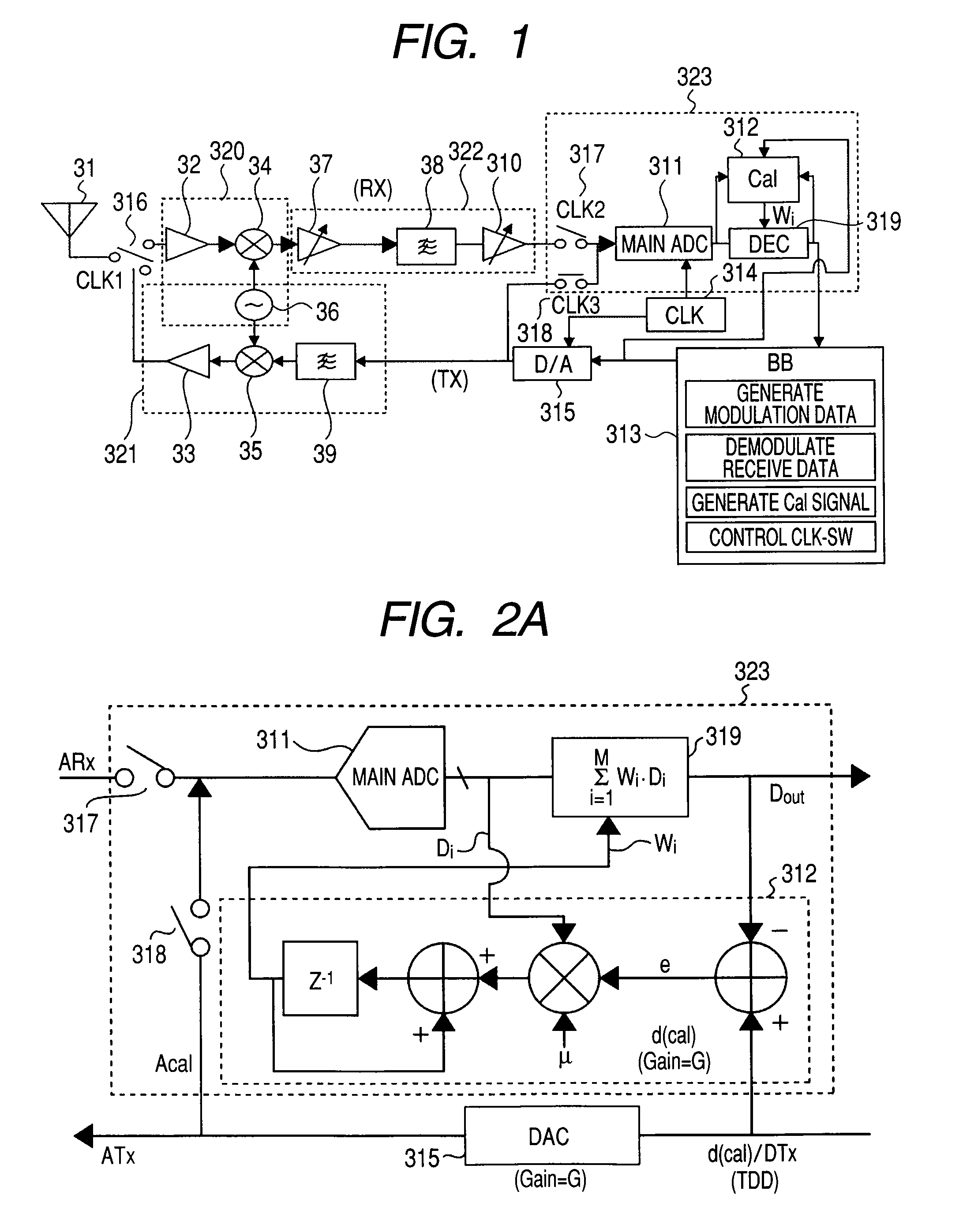
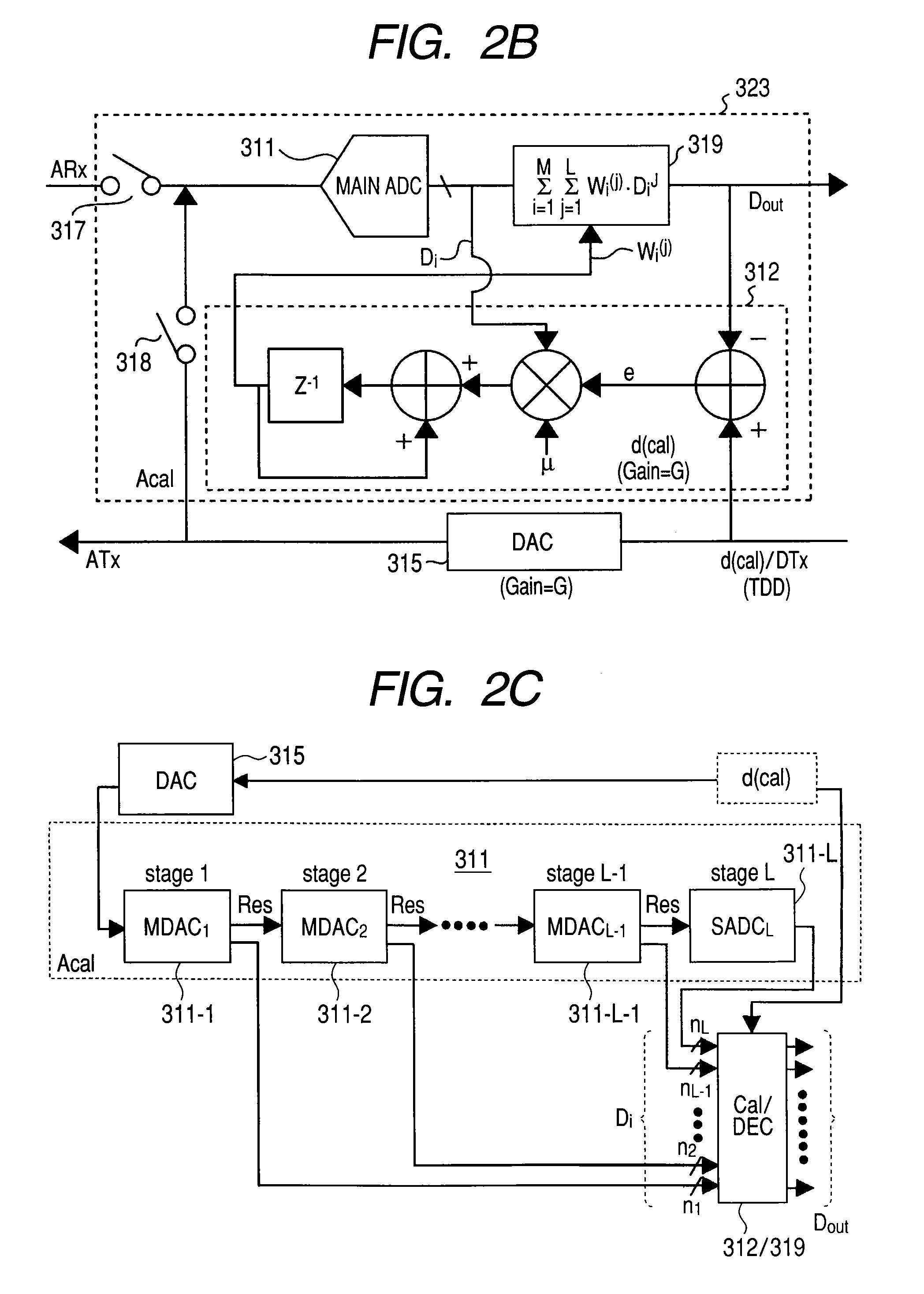
[0050]First, a basic configuration of a communication device including a foreground calibration type analog-to-digital converter according to a first embodiment of the present invention will be described with reference to FIG. 1 to FIG. 4.

[0051]FIG. 1 is a view showing an entire circuit configuration of the present invention applied to a wireless transmitter and receiver. In FIG. 1, the wireless transmitter and receiver corresponds to a time division duplex (TDD) method and includes a first switch (CLK1) 316 that switches a transmitting and receiving system to an antenna 31. A receiver circuit RX includes: an RF section 320 for reception that is connected to the first switch, an intermediate frequency processing section 322 that is connected to an output of the RF section for reception; and a foreground calibration type analog-to-digital converter 323 that is connected to an output of the intermediate frequency signal processing section via a second switch (CLK2) 317. The output ter...

second embodiment

[0088]Next, a basic configuration of a communication device including a foreground calibration type analog-to-digital converter according to a second embodiment of the present invention will be described with reference to FIGS. 5 and 6. FIG. 5 shows the entire circuit configuration of the wireless transmitter and receiver to which the present invention is applied. FIG. 6 is a time chart showing the operation of the calibration type analog-to-digital converter 323.

[0089]The baseband signal processing section 313 includes a modulation data generating function that generates a modulation data for modulating the transmission frequency, a receiving data demodulation function that demodulates and codes the receiving data, and a CLK switch control function that controls CLK switches (CLK 1 to 3). In the second embodiment, the transmission received is also used in the digital calibration signal d(cal). For this reason, the baseband signal processing section 313 does not have the function th...

third embodiment

[0098]Next, a basic configuration of a communication device including a foreground calibration type analog-to-digital converter according to a third embodiment of the present invention will be described with reference to FIGS. 7 and 8. FIG. 7 shows the entire circuit configuration of the wireless transmitter and receiver to which the present invention is applied. Although the basic configuration and operation of the third embodiment is the same as the second embodiment, in the third embodiment, a variable gain amplifier 340 is inserted between the output of the digital-to-analog converter 315 and the input of the analog-to-digital converter 324. By such a configuration, the signal level input to the analog-to-digital converter 324 can be optimally controlled.

[0099]In FIG. 7, at the time of transmission, the first switch 316 is connected to the RF section 320 for transmission, the second switch317 is opened, and the third switch 318 is closed, such that the output of the variable gai...


PUM


Abstract

In a wireless transmitter and receiver, a background calibration type analog-to-digital converter generally occupies a large area because of the phase compensating capacity of an op-amp included in a reference analog-to-digital conversion unit. Further, the calibration type analog-to-digital converter generally requires a sample and hold circuit to exclude influence of parasitic capacitance of wirings, thereby increasing power consumption. Digital calibration is performed by using, as a signal for calibration, an input signal of a digital-to-analog converter in a transmitter circuit of the wireless transmitter and receiver and inputting an output signal from the digital-to-analog converter to the analog-to-digital converter in the receiver circuit.

Description

CLAIM OF PRIORITY[0001]The present application claims priority from Japanese Patent Application JP 2007-336692 filed on Dec. 27, 2007, the content of which is hereby incorporated by reference into this application.FIELD OF THE INVENTION[0002]The present invention relates to an analog-to-digital converter and a communication device and a wireless transmitter and receiver using the same, and more particularly, to an analog-to-digital converter that has a function of using a digital signal to calibrate an output of the analog-to-digital converter and a wired and wireless communication device and a wireless transmitter and receiver using the same.BACKGROUND OF THE INVENTION[0003]A communication device, for example, an analog-to-digital converter, which is mounted on a radio device (wireless transmitter and receiver), has a calibration function to prevent its own characteristics from changing, even when there is a change in the environment, such as deviations in manufacturing processes, ...

Claims


Application Information

Patent Timeline
Patent Type & Authority Patents(United States)
IPC IPC(8): H03M1/10H04B1/40
CPCH03M1/1033H03M1/12
Inventor TAKAHASHI, TOMOMIOSHIMA, TAKASHIYAMAWAKI, TAIZO
Owner HITACHI LTD
Why Eureka
Try Eureka