Analog-to-digital converter and communication device and wireless transmitter and receiver using the same
a technology of analog-to-digital converter and communication device, which is applied in the direction of code conversion, transmission systems, instruments, etc., can solve the problems of increasing power consumption and achieve the effect of reducing the circuit area
- Summary
- Abstract
- Description
- Claims
- Application Information
AI Technical Summary
Benefits of technology
Problems solved by technology
Method used
Image
Examples
first embodiment
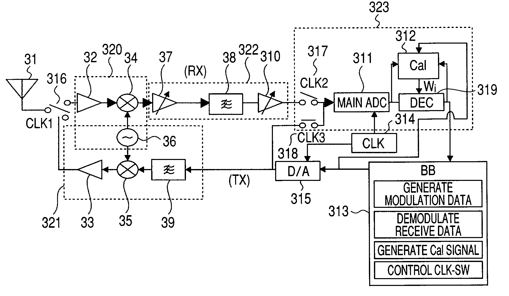
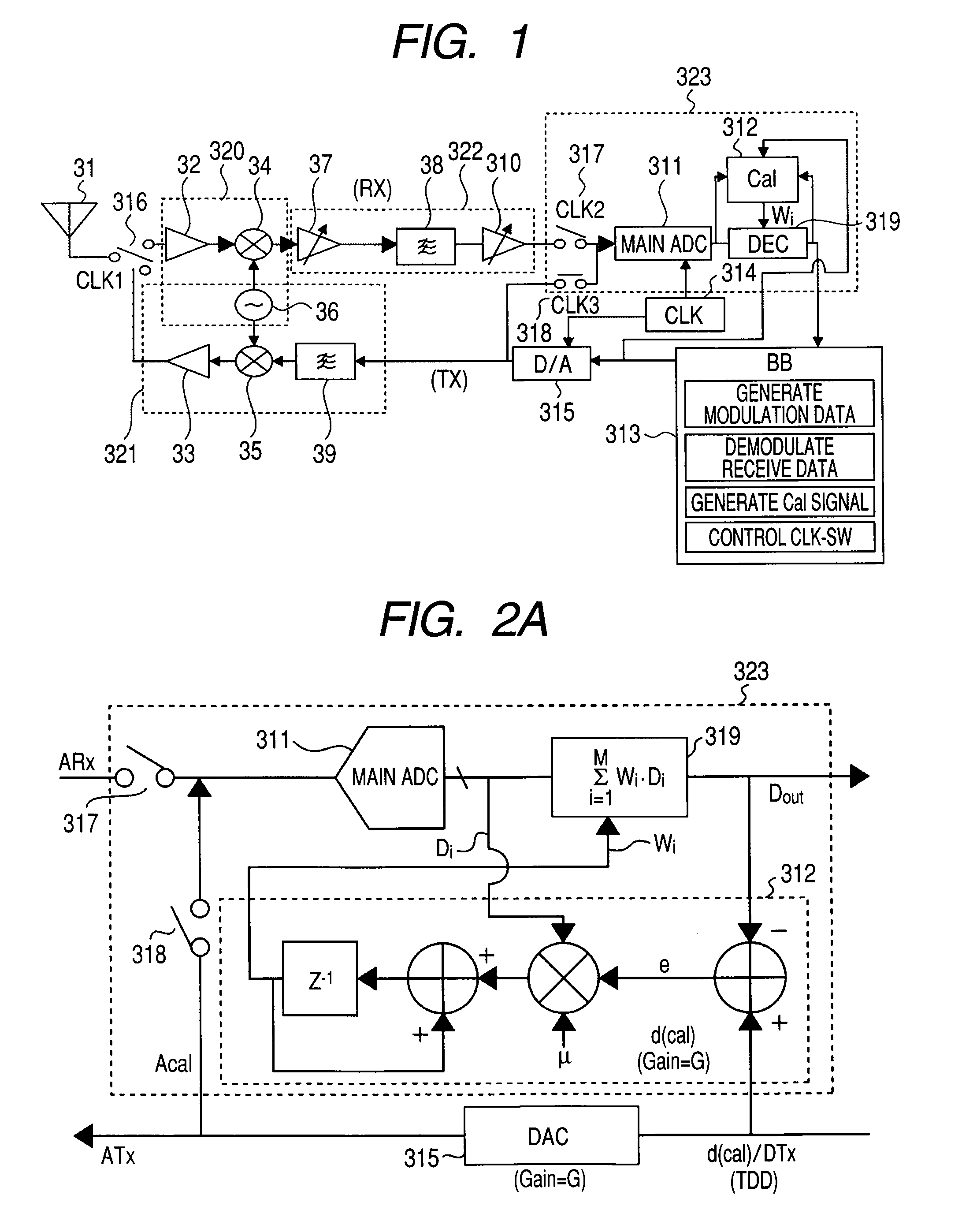
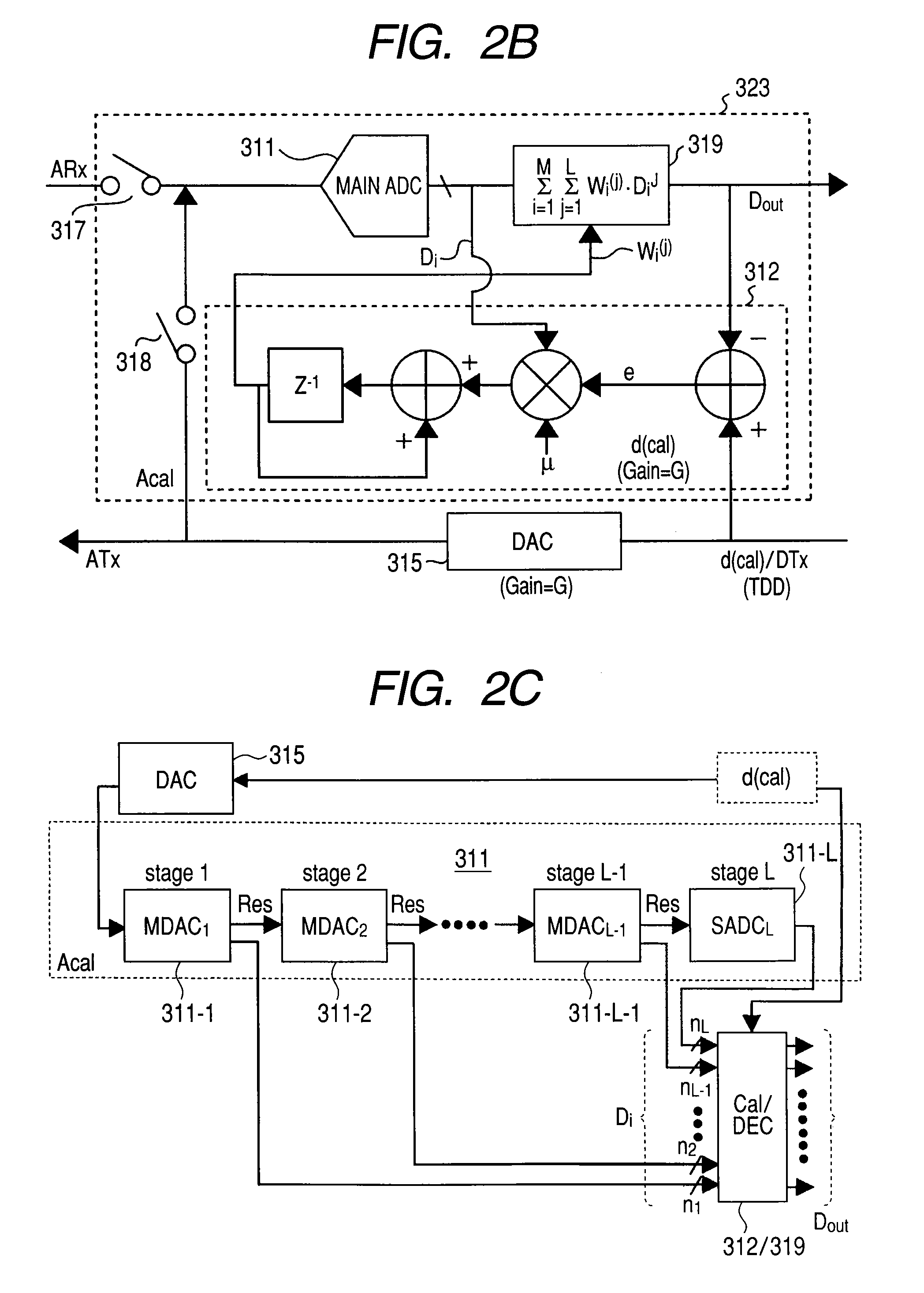
[0050]First, a basic configuration of a communication device including a foreground calibration type analog-to-digital converter according to a first embodiment of the present invention will be described with reference to FIG. 1 to FIG. 4.
[0051]FIG. 1 is a view showing an entire circuit configuration of the present invention applied to a wireless transmitter and receiver. In FIG. 1, the wireless transmitter and receiver corresponds to a time division duplex (TDD) method and includes a first switch (CLK1) 316 that switches a transmitting and receiving system to an antenna 31. A receiver circuit RX includes: an RF section 320 for reception that is connected to the first switch, an intermediate frequency processing section 322 that is connected to an output of the RF section for reception; and a foreground calibration type analog-to-digital converter 323 that is connected to an output of the intermediate frequency signal processing section via a second switch (CLK2) 317. The output ter...
second embodiment
[0087]Next, a basic configuration of a communication device including a foreground calibration type analog-to-digital converter according to a second embodiment of the present invention will be described with reference to FIGS. 5 and 6. FIG. 5 shows the entire circuit configuration of the wireless transmitter and receiver to which the present invention is applied. FIG. 6 is a time chart showing the operation of the calibration type analog-to-digital converter 323.
[0088]The baseband signal processing section 313 includes a modulation data generating function that generates a modulation data for modulating the transmission frequency, a receiving data demodulation function that demodulates and codes the receiving data, and a CLK switch control function that controls CLK switches (CLK 1 to 3). In the second embodiment, the transmission received is also used in the digital calibration signal d(cal). For this reason, the baseband signal processing section 313 does not have the function th...
third embodiment
[0097]Next, a basic configuration of a communication device including a foreground calibration type analog-to-digital converter according to a third embodiment of the present invention will be described with reference to FIGS. 7 and 8. FIG. 7 shows the entire circuit configuration of the wireless transmitter and receiver to which the present invention is applied. Although the basic configuration and operation of the third embodiment is the same as the second embodiment, in the third embodiment, a variable gain amplifier 340 is inserted between the output of the digital-to-analog converter 315 and the input of the analog-to-digital converter 324. By such a configuration, the signal level input to the analog-to-digital converter 324 can be optimally controlled.
[0098]In FIG. 7, at the time of transmission, the first switch 316 is connected to the RF section 320 for transmission, the second switch 317 is opened, and the third switch 318 is closed, such that the output of the variable ga...
PUM
 Abstract
Description
Claims
Application Information


