Solid state imaging device in which a plurality of imaging pixels are arranged two-dimensionally, and a manufacturing method for the solid state imaging device

a manufacturing method and imaging device technology, applied in the direction of color television, television system, radio control device, etc., can solve the problems of difficult to achieve a reduction in the thickness direction of the semiconductor substrate, difficult to reliably prevent stray light from entering adjacent imaging pixels, and difficult to achieve a reduction in the size of the thickness of the semiconductor substrate b>, and achieve the effect of easy manufacturing

Active Publication Date: 2010-12-07
CONVERSANT INTPROP MANAGEMENT INC
View PDF5 Cites 17 Cited by
  • Summary
  • Abstract
  • Description
  • Claims
  • Application Information

AI Technical Summary

Benefits of technology

[0011]The present invention has been achieved in view of the above problem, and an aim thereof is to provide a solid state imaging device that effectively suppresses occurrences of color mixing regardless of imaging pixel size, and a manufacturing method for the solid state imaging device.
[0016]In the solid state imaging device of the present invention, light is blocked by the light blocking portions even when passing through the optical filters, thereby eliminating the leakage of light into adjacent imaging pixels. This superior effect is achieved regardless of the size of the imaging pixel.
[0017]Accordingly, the solid state imaging device of the present invention effectively suppresses color mixing regardless of the size of imaging pixels.
[0031]The manufacturing method for the solid state imaging device of the present invention enables easily manufacturing the solid state imaging device of the present invention.

Problems solved by technology

However, reliably preventing stray light from entering adjacent imaging pixels is difficult, even when the structure proposed in Japanese Patent Application Publication No. 2001-77339 is used.
Such color mixing is particularly problematic in view of progress in reducing the size of imaging pixels while increasing the number of pixels.
This problem arises from the fact that it is much more difficult to achieve a reduction in size in the thickness direction of the semiconductor substrate 900 than in a direction along the arrangement of the photodiodes 901.

Method used


Image

  • Solid state imaging device in which a plurality of imaging pixels are arranged two-dimensionally, and a manufacturing method for the solid state imaging device
  • Solid state imaging device in which a plurality of imaging pixels are arranged two-dimensionally, and a manufacturing method for the solid state imaging device
  • Solid state imaging device in which a plurality of imaging pixels are arranged two-dimensionally, and a manufacturing method for the solid state imaging device

Examples


embodiment 1

[0052]1. Overall Structure

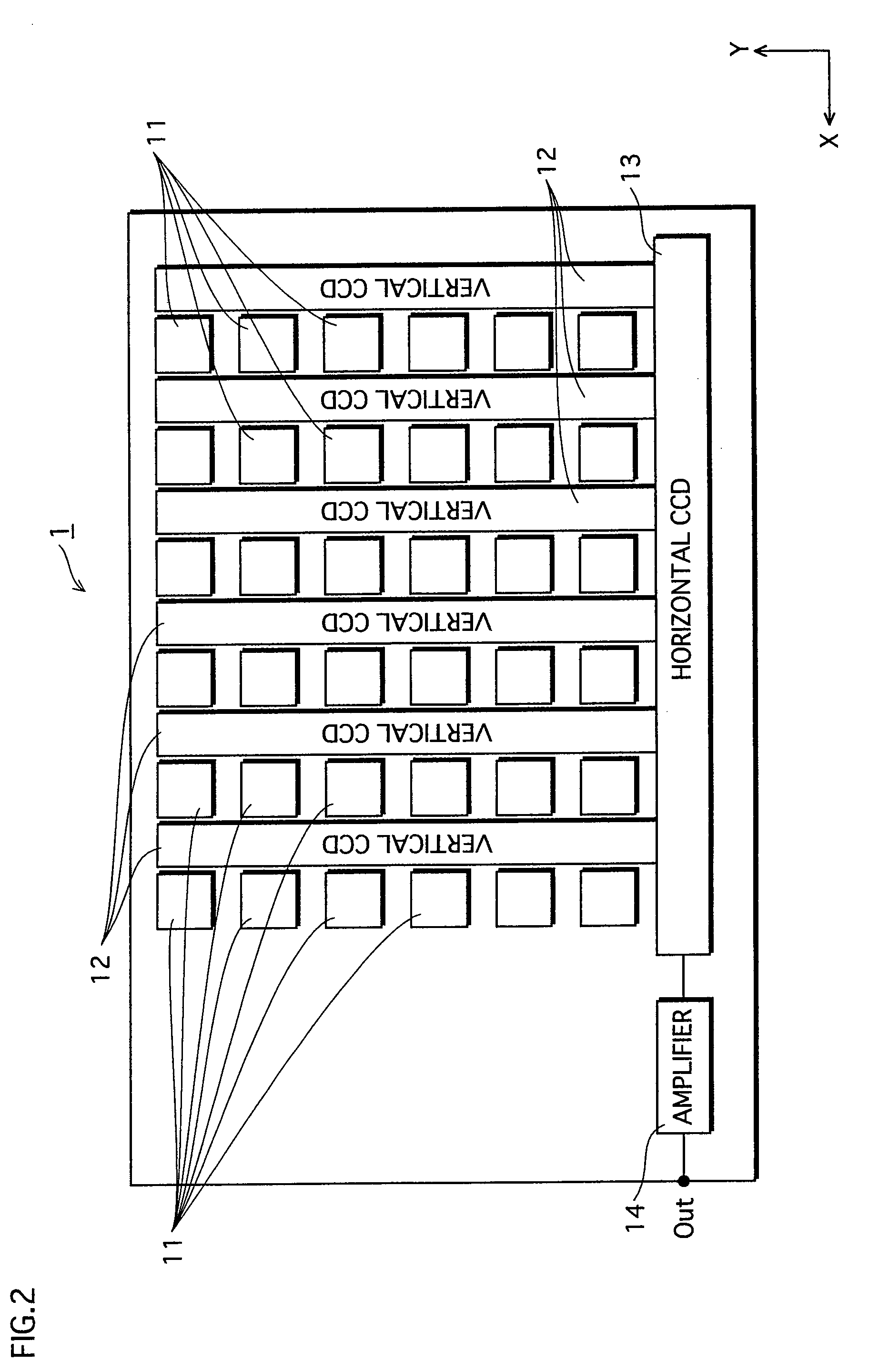
[0053]The following describes the overall structure of a solid state imaging device 1 of the present embodiment with reference to FIG. 2.

[0054]As shown in FIG. 2, the solid state imaging device 1 is made up of a plurality of imaging pixels 11 arranged in a matrix and circuitry. The circuitry includes vertical CCDs 12 that are arranged extending in the Y axis direction between adjacent columns of imaging pixels 11, a horizontal CCD 13 arranged extending in the X axis direction, and an amplifier 14 connected to the horizontal CCD 13. Although the structure of an interline (IT) CCD type of solid state imaging device is described in the present embodiment, this is merely one example.

[0055]The vertical CCDs 12 receive signal charges generated by photoelectric converters on which light has incidented, and transfer the signal charges downward in the Y axis direction. The signal charges in the vertical CCDs 12 are transferred to the horizontal CCD 13 sequentially a...

embodiment 2

[0080]1. Structure of Imaging Pixels and Vertical CCDs

[0081]The following describes the structure of a solid state imaging device 2 pertaining to embodiment 2 with reference to FIG. 6. The solid state imaging device 2 of the present embodiment differs from the solid state imaging device 1 of embodiment 1 with respect to the position of the top edges of light blocking walls 213 and the configuration of portions in the vicinity. The following description focuses on these differences.

[0082]As shown in FIG. 6, in the solid state imaging device 2, the top edges of the light blocking walls 213 are higher than the top faces of planarizing films 211. Specifically, in the solid state imaging device 2, the top edges of the light blocking walls 213 are in contact with top lenses 212, and the planarizing films 211 in the imaging pixels are separated from each other by the light blocking walls 213. A description of other portions of the structure has been omitted due to being the same as the sol...
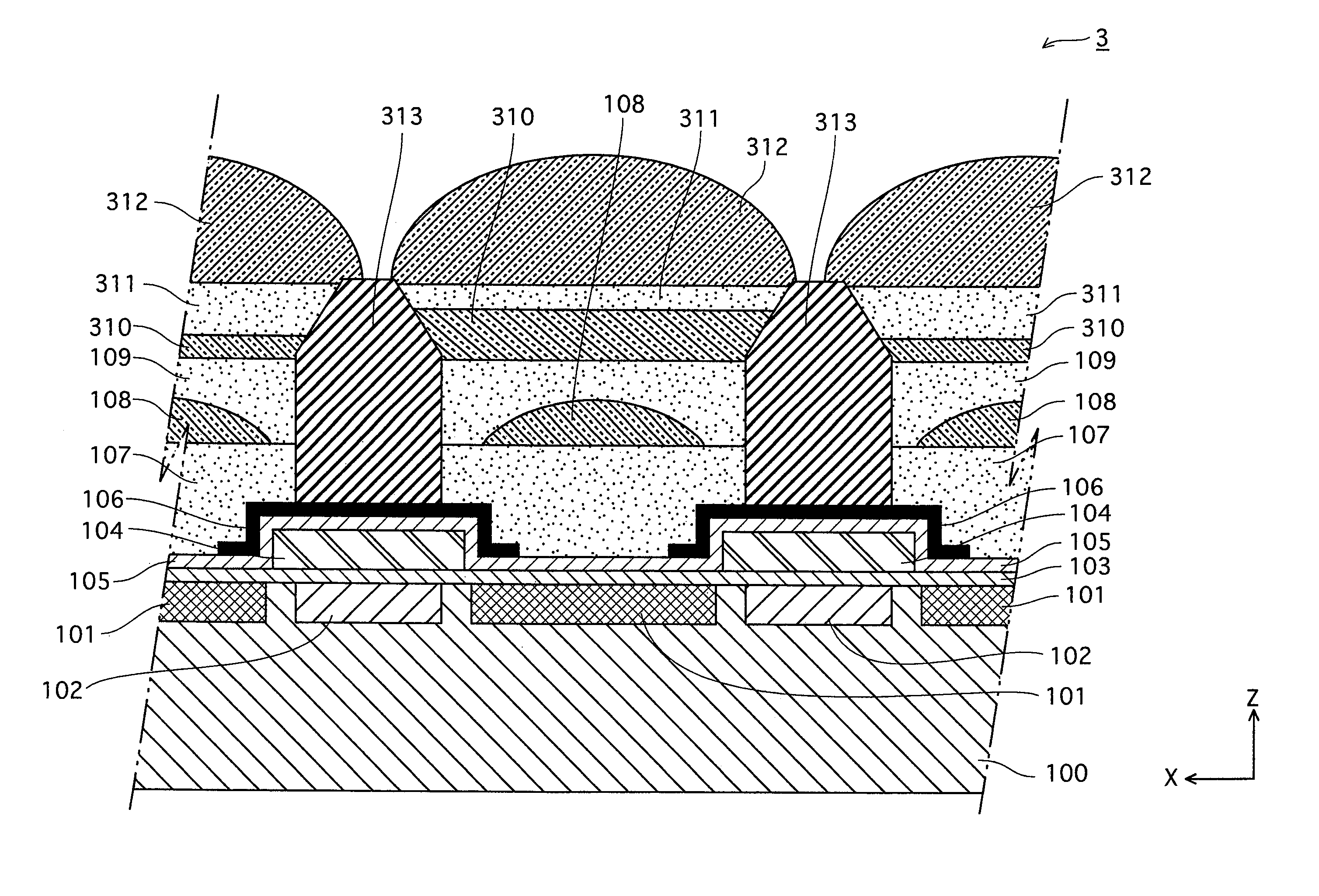
embodiment 3

[0091]1. Structure of Imaging Pixels and Vertical CCDs

[0092]The following describes the structure of a solid state imaging device 3 pertaining to embodiment 3 with reference to FIG. 8. The solid state imaging device 3 differs from the solid state imaging device 2 only with respect to the configuration of the top edge portions of light blocking walls 313.

[0093]As shown in FIG. 8, in the solid state imaging device 3, the configuration of the top edge portions of the light blocking walls 313 is such that from above the lower faces of color filters 310, the cross-sectional area of the top edge portions decreases in the upward direction. More specifically, the top edge portions of the light blocking walls 313 have a trapezoidal shape. The trapezoidal portion may specifically be such that, for example, the taper angle of the lateral faces is 1[°] to 30[°], or the top edge of the trapezoidal portion fits between adjacent top lenses 312.

[0094]The light blocking walls 313 of the solid state ...


PUM


Abstract

A solid state imaging device includes a plurality of imaging pixels that are arranged two-dimensionally along a main face of a semiconductor substrate. Each imaging pixel in the solid state imaging device includes a photodiode that performs photoelectric conversion and a color filter that is disposed higher in the Z axis direction than the photodiode. Also, light blocking portions have been formed between pairs of adjacent imaging pixels, on the main face of the semiconductor substrate to a height in a thickness direction (Z axis direction) of the semiconductor substrate that is substantially equal to or higher than top edges of the optical filters. Each light blocking portion is constituted from a combination of a light blocking film and a light blocking wall.

Description

BACKGROUND OF THE INVENTION[0001]1. Field of the Invention[0002]The present invention relates to a solid state imaging device and a manufacturing method for the same, and in particular to technology for blocking light between adjacent imaging pixels.[0003]2. Description of the Related Art[0004]In recent years, solid state imaging devices have been used in a wide range of devices including digital video cameras, digital still cameras, and mobile phones. One structure of a solid state imaging device is described below with reference to FIG. 1. The solid state imaging device shown in FIG. 1 is proposed in Japanese Patent Application Publication No. 2001-77339, and aims to suppress color mixing etc.[0005]As shown in FIG. 1, the solid state imaging device includes a semiconductor substrate 900 and a gate insulation film 903 that has been formed on a main face thereof (in FIG. 3, the upper face in the Z axis direction). Photodiodes 901 having gaps therebetween have been formed at a bounda...

Claims


Application Information

Patent Timeline
Patent Type & Authority Patents(United States)
IPC IPC(8): H01L31/0232H01L27/14H04N5/335H04N5/357
CPCH01L27/14843H01L31/02162H01L31/02164H01L27/14623H01L27/14627
Inventor KOKUSENYA, NOBORU
Owner CONVERSANT INTPROP MANAGEMENT INC
Why Eureka
Try Eureka