
Driving circuit for power semiconductor element including controlling circuit that provides control when detected voltage reaches predetermined voltage

a technology of driving circuit and semiconductor element, applied in the direction of pulse technique, oscillation generator, power conversion system, etc., can solve the problems of large sensor size, low precision of hall magnetic sensor and single magnetic resistance element, and high cost, so as to reduce surge voltage and switching loss

Inactive Publication Date: 2010-12-07
TOYOTA JIDOSHA KK
View PDF14 Cites 3 Cited by
  • Summary
  • Abstract
  • Description
  • Claims
  • Application Information

AI Technical Summary

Benefits of technology

[0006]The present invention provides a driving circuit which can reduce surge voltage and switching loss during switching of a semiconductor element for power.
[0011]According to various aspects of the present invention, it is possible to inhibit surge voltage and reduce switching loss during turn-off or turn-on with a high precision, even with a simple structure.

Problems solved by technology

However, when the element current is to be detected, flux-concentration type magnetic current sensors have problems in that they are costly and the sensor size is large.
Hall magnetic sensors and single magnetic resistance elements have inferior precision and are also costly.
However, it is difficult to achieve both precision and high speed detection at the same time.
In addition, when the gate voltage is to be detected, there also are problems in that the gate voltage shows complex behaviors because feedback is applied from a parasitic capacitance of the driving element during switching, and that switching noise from other circuits connected to the same ground line tends to mix because the power supply is approximately 15V.
However, because the voltage differential signal has a small value, a large control error is caused by other noise, and thus the voltage differential signal is unsuited as a control signal during switching.
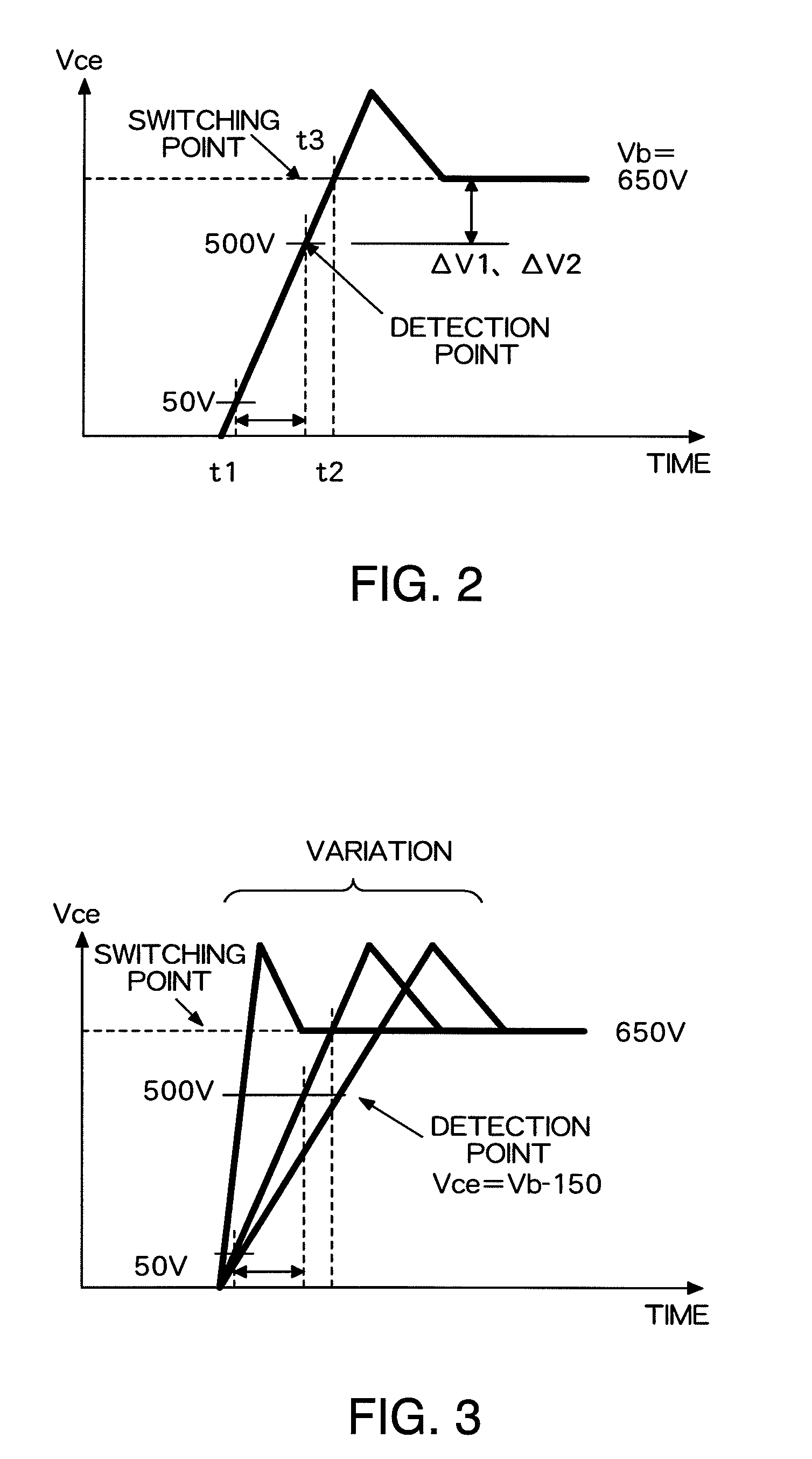
However, in Patent Reference 1, there is no disclosure of the detection point and, in Patent Reference 2, a point in which the element voltage is low is set as the detection point and there is a problem in that variation of elements cannot be handled.

Method used


Image

  • Driving circuit for power semiconductor element including controlling circuit that provides control when detected voltage reaches predetermined voltage
  • Driving circuit for power semiconductor element including controlling circuit that provides control when detected voltage reaches predetermined voltage
  • Driving circuit for power semiconductor element including controlling circuit that provides control when detected voltage reaches predetermined voltage

Examples


Embodiment Construction

[0026]A preferred embodiment of the present invention will now be described in detail with reference to the drawings.

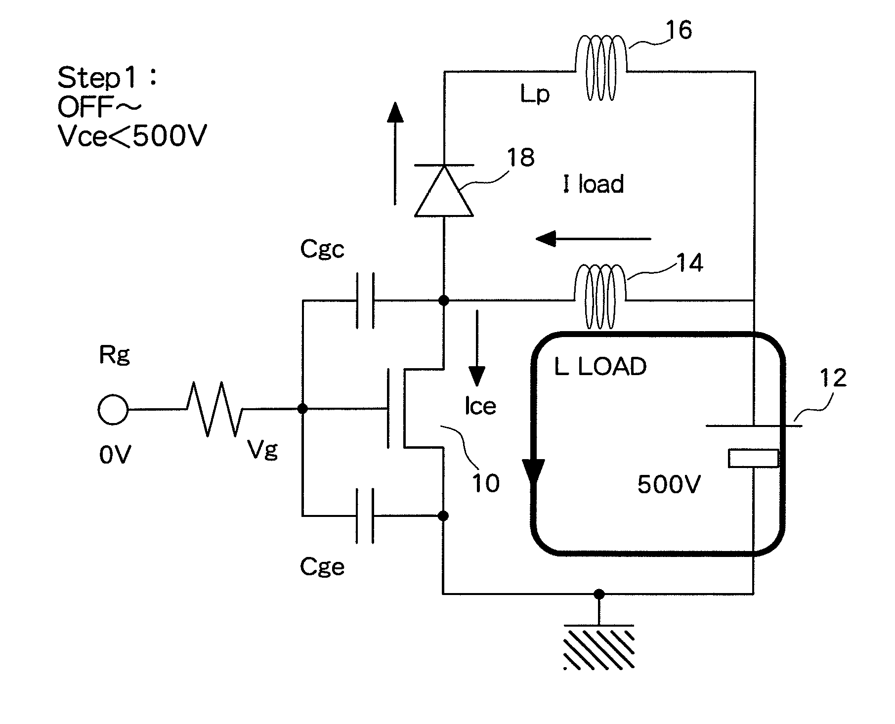
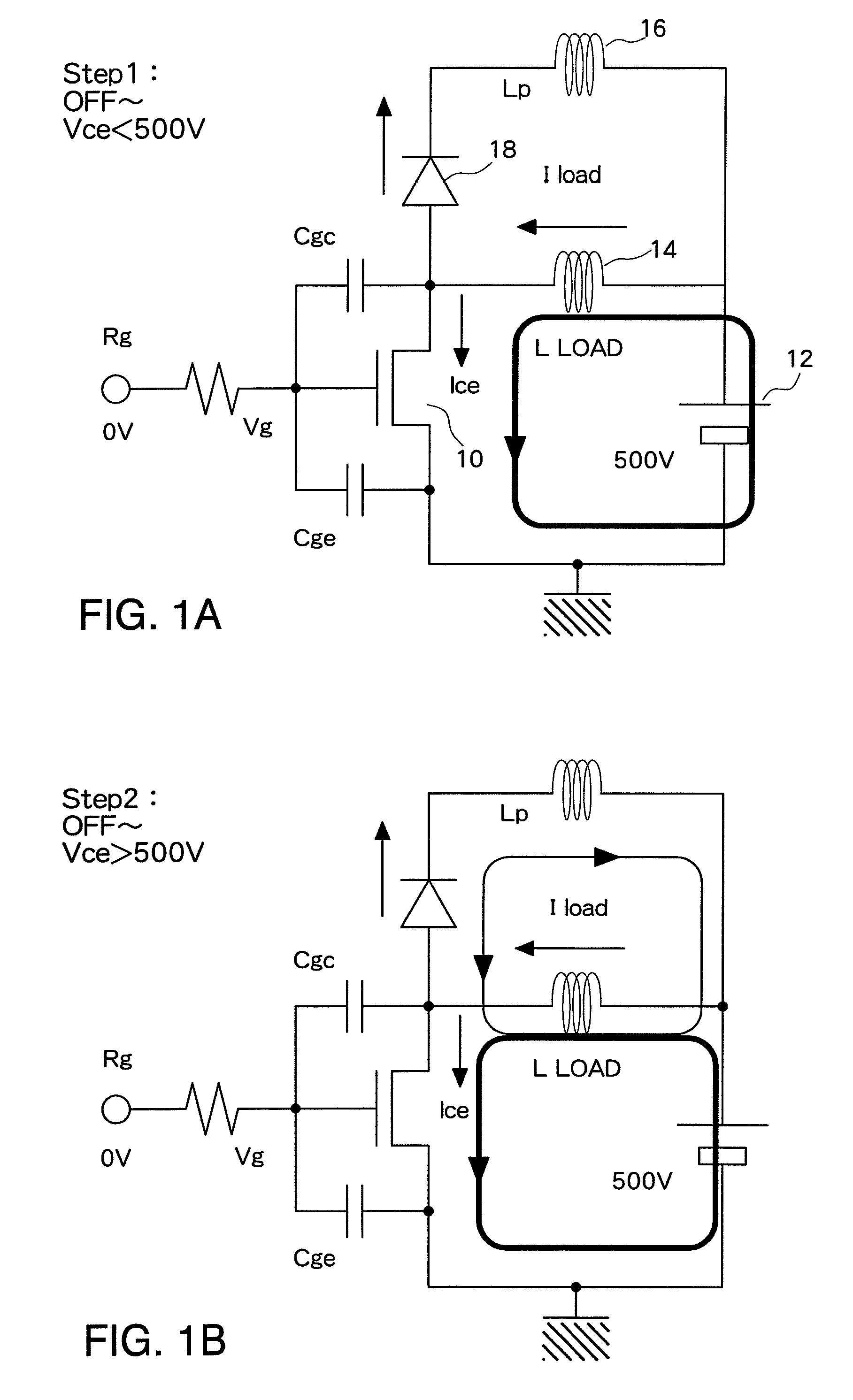
[0027]A turn-off during drive of an inductance load (L) using a MOSFET or an IGBT as a semiconductor element for power (power semiconductor) will first be described. FIG. 1A and FIG. 1B show a circuit structure. An element 10 to be driven and a diode 18 are connected in series to a power supply 12. An inductance load (L) 14 is connected between a connecting point between the element 10 to be driven and the diode 18 and the power supply 12. In a case of a large load L, as shown in step 1 of FIG. 1A, the same element current Ice continues to flow even when a gate voltage Vg of the element 10 to be driven is set to an OFF level. When the element voltage of the element 10 to be driven exceeds the power supply voltage of the power supply 12 (500 V in FIG. 1), as shown in step 2 in FIG. 1B, current starts to flow in the diode 18 which is connected in series, and the element...


PUM


Abstract

Provided is a driving circuit which suppresses a surge voltage at the time of switching a power semiconductor element and reduces switching loss. An element (10) such as an IGBT and another element (20) to be paired are connected, the element (10) is driven by a driver (22), and a gate voltage is controlled by a control circuit (24). When the power semiconductor element is turned off, a comparator (26) detects that a voltage (Vak) of the element (20) is a prescribed voltage, the control circuit (24) switches gate resistance from low resistance to high resistance to suppress the surge voltage, and the switching loss is reduced. When the power semiconductor element is turned on, start up of the voltage (Vak) is detected, and the control circuit (24) switches the gate resistance from high resistance to low resistance after a prescribed time to suppress the surge voltage, and the switching loss is reduced.

Description

TECHNICAL FIELD[0001]The present invention relates to a driving circuit of a semiconductor element, and in particular, to reduction in surge voltage and in switching loss in a semiconductor element for power.BACKGROUND ART[0002]In a power circuit, a semiconductor switching element is used, and reductions in surge voltage during switching and in switching loss are important subjects. In the related art, methods are proposed in which gate voltage during switching of the semiconductor switching element is actively controlled so that switching loss is reduced while the surge voltage is maintained at a low level. In these methods, an element voltage, an element current, and a gate voltage of the switching element to be driven are detected, and a logic process is applied by a single detection signal or combination of detection signals, to control the gate voltage. The gate voltage is controlled by changing the voltage of the gate circuit or changing the gate resistance. Japanese Patent No...

Claims


Application Information

Patent Timeline
Patent Type & Authority Patents(United States)
IPC IPC(8): H03K3/00
CPCH02M1/08H03K17/0828H03K17/165H03K17/18H03K2217/0036
Inventor FUMA, HIROOKUNO, HIROMICHIHIROSE, SATOSHITAKAMATSU, NAOYOSHI
Owner TOYOTA JIDOSHA KK
Learn More