Single transistor memory device having source and drain insulating regions and method of fabricating the same

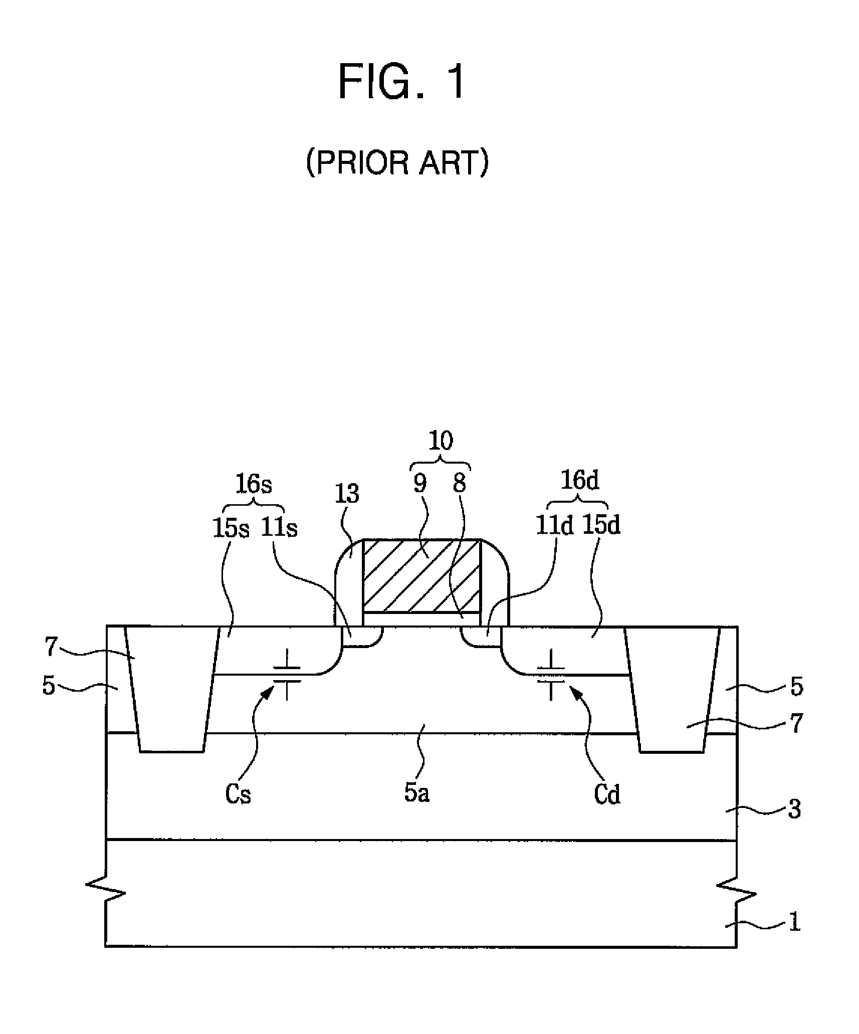
a single transistor and memory device technology, applied in semiconductor devices, semiconductor/solid-state device details, electrical apparatus, etc., can solve the problems of reducing the data sensing margin and operating speed the data retention characteristics of the single transistor dram cell illustrated in fig. 1 are poor, and the technology of highly integrated dram cells is limited

Active Publication Date: 2010-12-14
SAMSUNG ELECTRONICS CO LTD
View PDF46 Cites 17 Cited by
  • Summary
  • Abstract
  • Description
  • Claims
  • Application Information

AI Technical Summary

Problems solved by technology

That is, as many DRAM cells as possible are formed within a restricted space However, the technology of highly integrating DRAM cells faces several limitations.
In other words, the single transistor DRAM cell illustrated in FIG. 1 has poor data retention characteristics.
Thus, a loading capacitance of a bit line electrically connected to the drain region 16d increases, which may lead to a decrease in a data sensing margin and operating speed of the single transistor DRAM cell.

Method used


Image

  • Single transistor memory device having source and drain insulating regions and method of fabricating the same
  • Single transistor memory device having source and drain insulating regions and method of fabricating the same
  • Single transistor memory device having source and drain insulating regions and method of fabricating the same

Examples


Embodiment Construction

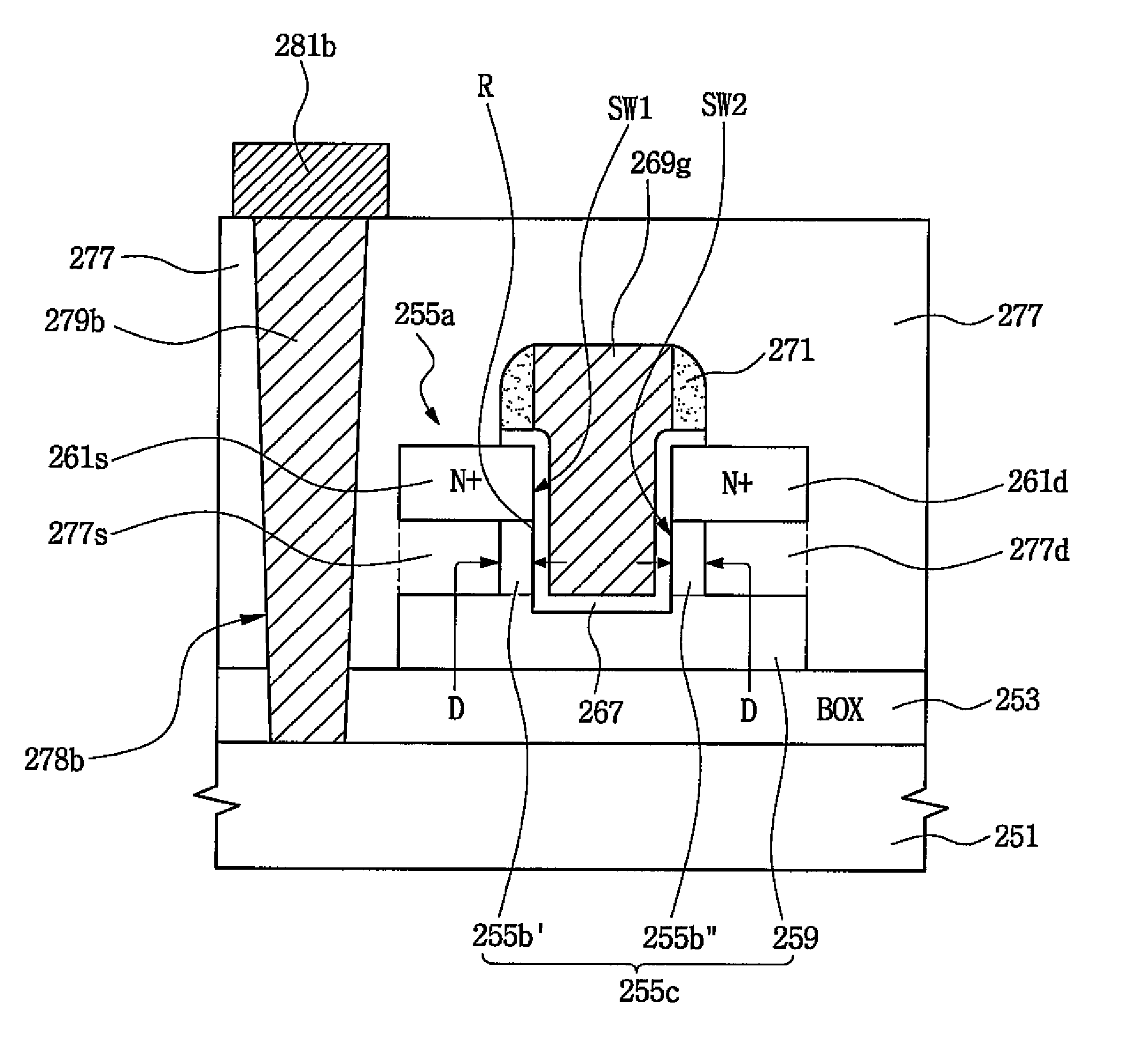
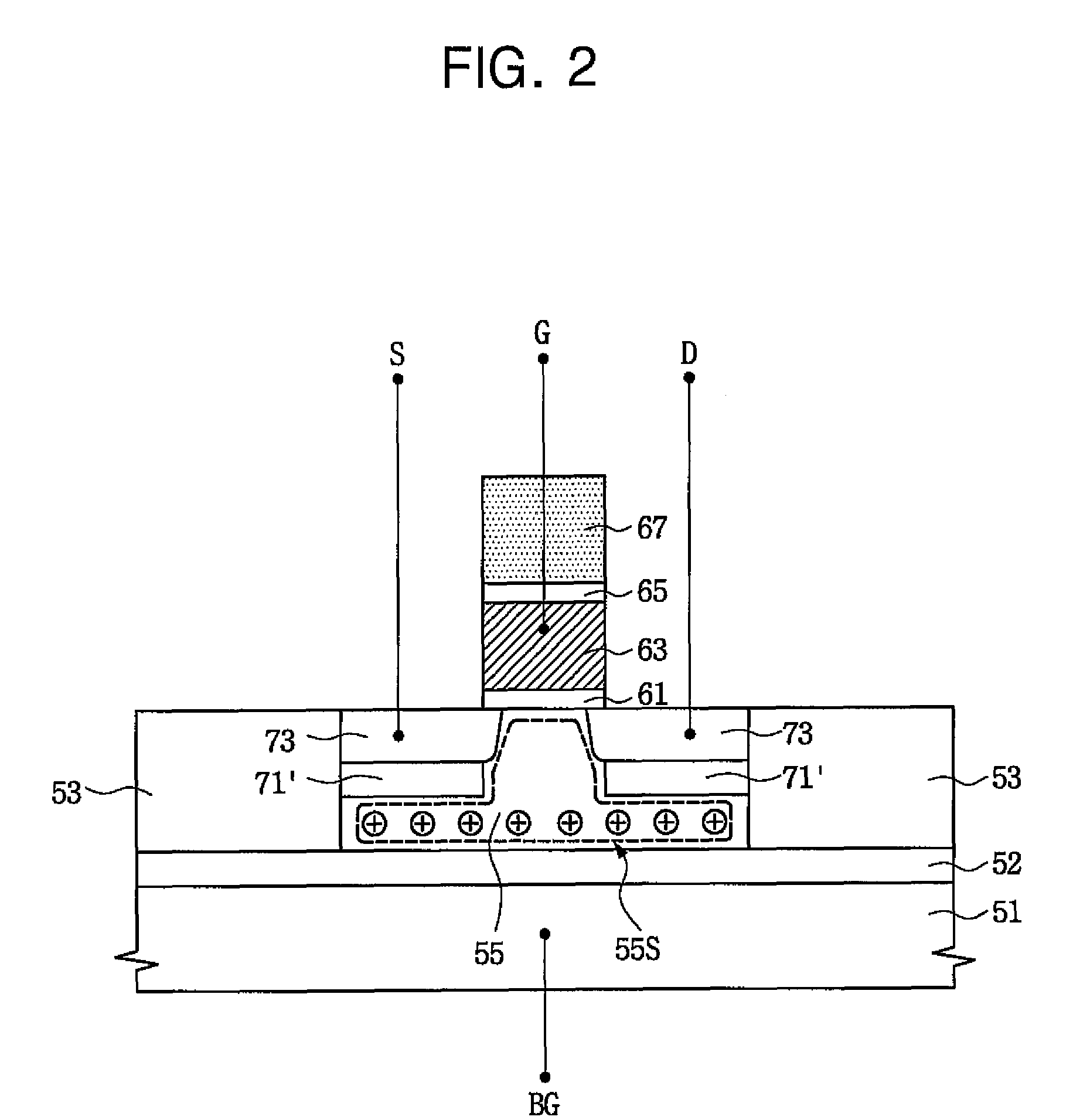
[0036]The present invention will now be described more fully with reference to the accompanying drawings, in which exemplary embodiments of the invention are shown. The invention, however, may be embodied in various different forms, and should not be construed as being limited only to the illustrated embodiments. Rather, these embodiments are located as examples, to convey the concept of the invention to one skilled in the art. Accordingly, known processes, elements, and techniques are not described with respect to some of the embodiments of the present invention. Throughout the drawings and written description, like reference numerals will be used to refer to like or similar elements.

[0037]In the drawings, the thickness of layers and regions may be exaggerated for clarity. Also, when a layer is described to be formed on other layer or on a substrate, this means that the layer may be formed on the other layer or on the substrate, or a third layer may be positioned between the layer ...


PUM


Abstract

A single transistor floating-body dynamic random access memory (DRAM) device includes a floating body located on a semiconductor substrate and a gate electrode located on the floating body, the floating body including an excess carrier storage region. The DRAM device further includes source and drain regions respectively located at both sides of the gate electrode, and leakage shielding patterns located between the floating body and the source and drain regions. Each of the source and drain regions contact the floating body, which may be positioned between the source and drain regions. The floating body may also laterally extend under the leakage shielding patterns, which may be arranged at outer sides of the gate electrode.

Description

CROSS-REFERENCE TO RELATED APPLICATIONS[0001]A claim of priority is made to Korean Patent Application Nos. 10-2006-0107345 and 10-2006-0119087, filed on Nov. 1, 2006, and Nov. 29, 2006, respectively, the subject matters of which are hereby incorporated herein by reference.BACKGROUND OF THE INVENTION[0002]1. Field of the Invention[0003]The present invention relates to a semiconductor device and a method of fabricating the same. More particularly, the present invention relates to a single transistor memory device having insulating regions associated with the source and drain regions, and a method of fabricating the same.[0004]2. Description of the Related Art[0005]A conventional dynamic random access memory (DRAM) cell, which is a type of volatile memory, typically incorporates a capacitor, a transistor and interconnection units. In response to demands for electronic devices to be increasingly lightweight, small and thin, DRAM cells have become more highly integrated. That is, as many...

Claims


Application Information

Patent Timeline
Patent Type & Authority Patents(United States)
IPC IPC(8): H01L23/62
CPCH01L27/108H01L27/10802H01L29/0653H01L29/1045H01L29/7834H01L29/7841H10B12/20H10B12/00
Inventor TAK, NAM-KYUNSONG, KI-WHANOH, CHANG-WOOCHO, WOO-YEONG
Owner SAMSUNG ELECTRONICS CO LTD
Why Eureka
Try Eureka