

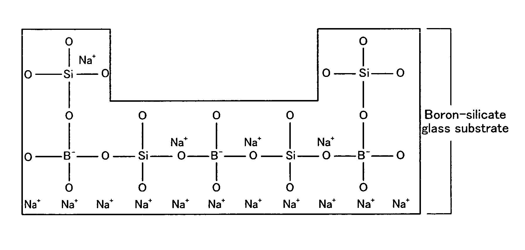
Nano fabrication method for glass
a technology of nano-fibre and glass, which is applied in the direction of decorative surface effects, electrical equipment, decorative arts, etc., can solve the problems of low productivity low production efficiency of electron beam lithography method, and inability to meet the needs of mass production, etc., and achieves the effect of easy and rapid processing
- Summary
- Abstract
- Description
- Claims
- Application Information
AI Technical Summary
Benefits of technology
Problems solved by technology
Method used
Image

Examples
experimental example 1
[0098]In Experimental Example 1, the thickness of the aluminum metal film pattern 2a on the Pyrex glass substrate 1 is selected as a variable. When the temperature and the applied current are constant, the Pyrex glass substrate 1 is patterned to have different pattern depths.
[0099]FIG. 6 is a drawing showing principal stages of a nano fabrication method for a glass according to Experimental Example 1.
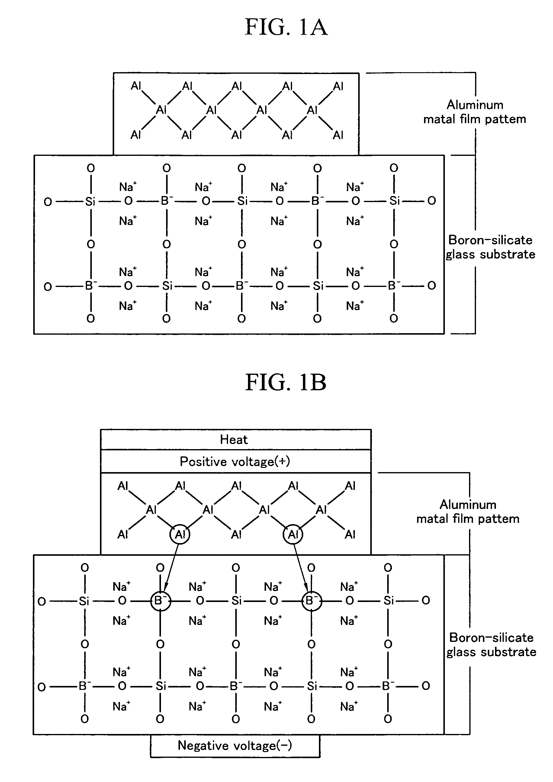
[0100]Referring to FIG. 6, the aluminum metal film pattern 2a is formed to have a step shape so as to have two different thicknesses.
[0101]During the molecule substituting step, aluminum atoms in the thicker portion of the aluminum metal film pattern 2a are more deeply substituted with boron atoms of the Pyrex glass substrate 1 rather than the thinner portion thereof.
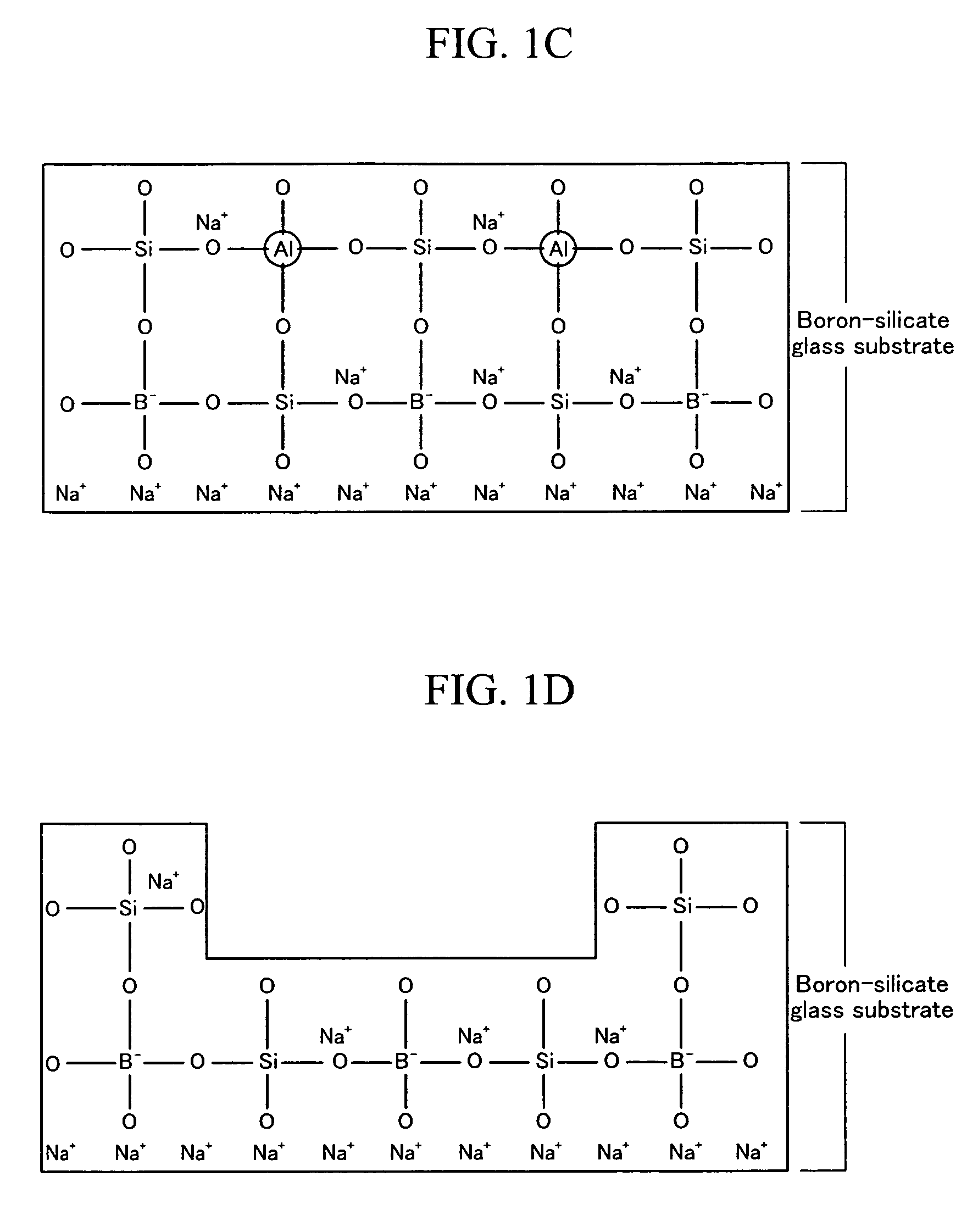
[0102]Subsequently, in the molecule substituting layer removing step, remaining aluminum metal film pattern 2a is removed from the Pyrex glass substrate 1.
[0103]And then, in the etching step, the Pyrex glass substrate 1 is ...
experimental example 2
[0107]In Experimental Example 2, the temperature of the heat treatment is selected as a variable. When the thickness of the aluminum metal film pattern 2a and the applied current are constant, the Pyrex glass substrate 1 is patterned to have different pattern depths.
[0108]FIG. 8 is a drawing showing principal stages of a nano fabrication method for a glass according to Experimental Example 2.
[0109]Referring to FIG. 8, aluminum metal film patterns 2a having the same thickness by a metal film forming step and a patterning step are formed on a Pyrex glass substrate 1.
[0110]In the molecule substituted step, electric fields of the same voltage of 1000V are applied to the patterns, and heat treatments are respectively performed to those patterns with different temperatures of 350° C., 400° C., 450° C., and 500° C., respectively.
[0111]After the metal film removing step and the etching step are performed, the pattern depth of the Pyrex glass substrate 1 is proportional to the heat treatment...
experimental example 3
[0116]In Experimental Example 3, the applied voltage of the electric filed is selected as a variable. When the thickness of the aluminum metal film pattern 2a and the heat treatment temperature of 500° C. are constant, the Pyrex glass substrate 1 is patterned to have different pattern depths.
[0117]FIG. 10 is a drawing showing principal stages of a nano fabrication method for a glass according to Experimental Example 3.
[0118]Referring to the drawing, in the molecule substituted step, the heat treatment temperature is maintained at 500° C., and different voltages of 700V, 800V, 900V, and 1000V are respectively applied to the pattern 2a.
[0119]After the metal film removing step and the etching step are performed, the pattern depth of the Pyrex glass substrate 1 is proportional to the applied voltage.
[0120]FIG. 11 is a collection of photographs showing results from a nano fabrication method for a glass according to the applied voltage of Experimental Example 3, and FIG. 12A to FIG. 12D ...
PUM
| Property | Measurement | Unit |
|---|---|---|
| temperature | aaaaa | aaaaa |
| size | aaaaa | aaaaa |
| thickness | aaaaa | aaaaa |
Abstract
Description
Claims
Application Information