Systems and methods for controlling the effective dielectric constant of materials used in a semiconductor device

a technology of effective dielectric constant and semiconductor device, which is applied in the direction of semiconductor device, semiconductor/solid-state device details, electrical apparatus, etc., can solve the problems of compromising reliability, poor strength characteristics, and significant challenges to the operation of high-performance circuits of dielectric layers

Inactive Publication Date: 2010-12-21
SEMATECH
View PDF12 Cites 7 Cited by
  • Summary
  • Abstract
  • Description
  • Claims
  • Application Information

AI Technical Summary

Benefits of technology

[0009]In yet another embodiment, a semiconductor device comprising a layer with reduced effective capacitance is fabricated by a method comprising the steps of: depositing a first layer of dielectric material over a semiconductor structure, where the first layer comprises a top portion having a top thickness deposited on top of each of a plurality of metal lines and a lateral portion having a lateral thickness deposited on sides of each of the plurality of metal lines, removing a lateral amount of dielectric material from the first layer approximately equal to the lateral thickness while leaving a top amount of dielectric material on top of each of the plurality of metal lines, and depositing a second dielectric layer over the semiconductor structure resulting in a plurality of voids between the plurality of metal lines that reduces an effective dielectric constant of the second dielectric layer.

Problems solved by technology

Although necessary to isolate the various metal layers, dielectric layers present significant challenges to the operation of high-performance circuits.
However, the inventor hereof has recognized that low-k materials are typically porous, have poor strength characteristics, and are more susceptible to damage, thus compromising their reliability.
These referenced shortcomings are not intended to be exhaustive, but rather are among many recognized by the present inventor that tend to impair the effectiveness of previously known techniques; however, those mentioned here are sufficient to demonstrate that the methodologies appearing in the art have not been satisfactory and that a significant need exists for the techniques described and claimed in this disclosure.

Method used


Image

  • Systems and methods for controlling the effective dielectric constant of materials used in a semiconductor device
  • Systems and methods for controlling the effective dielectric constant of materials used in a semiconductor device
  • Systems and methods for controlling the effective dielectric constant of materials used in a semiconductor device

Examples


Embodiment Construction

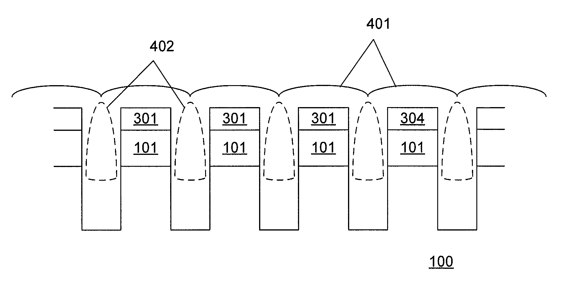
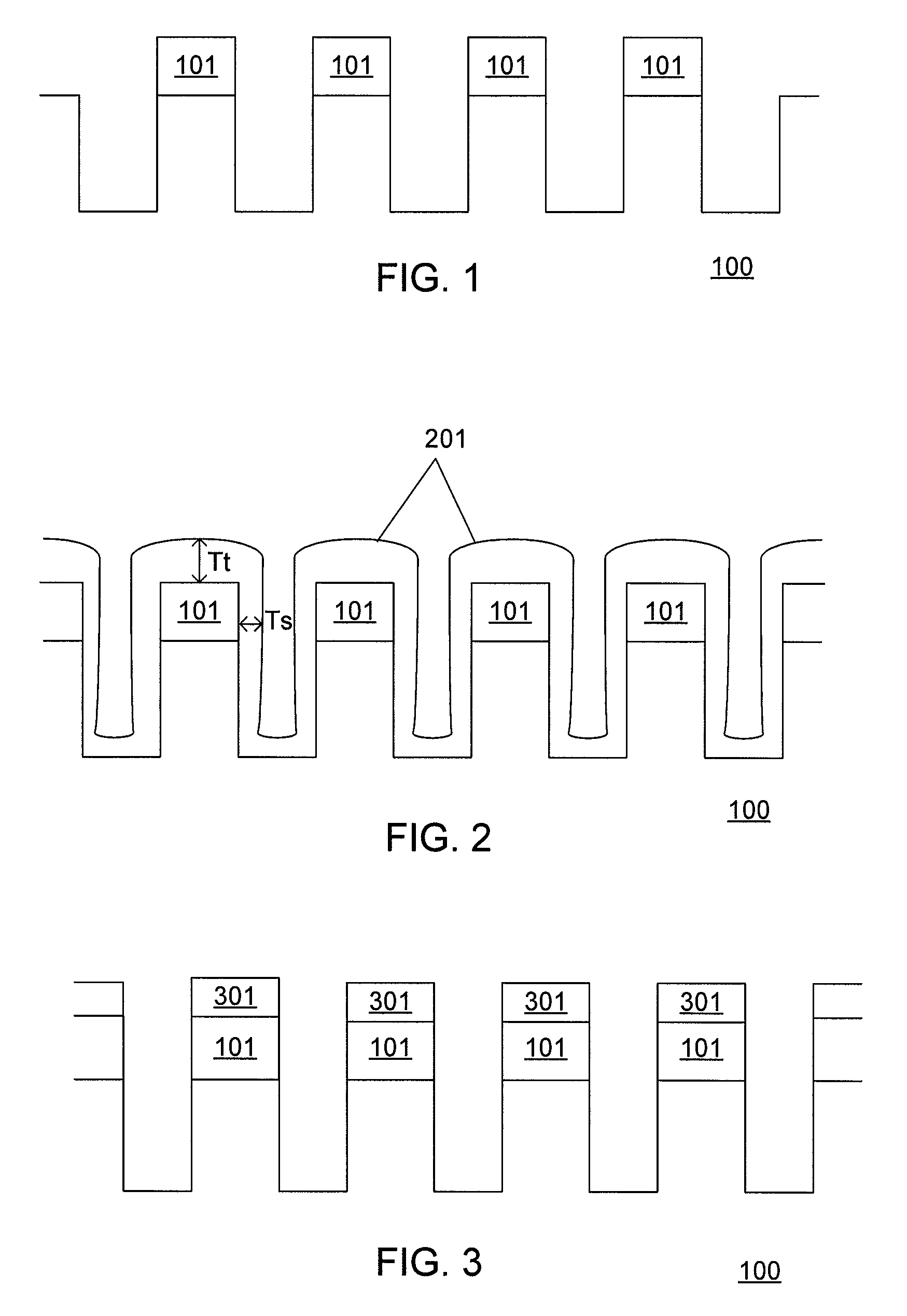
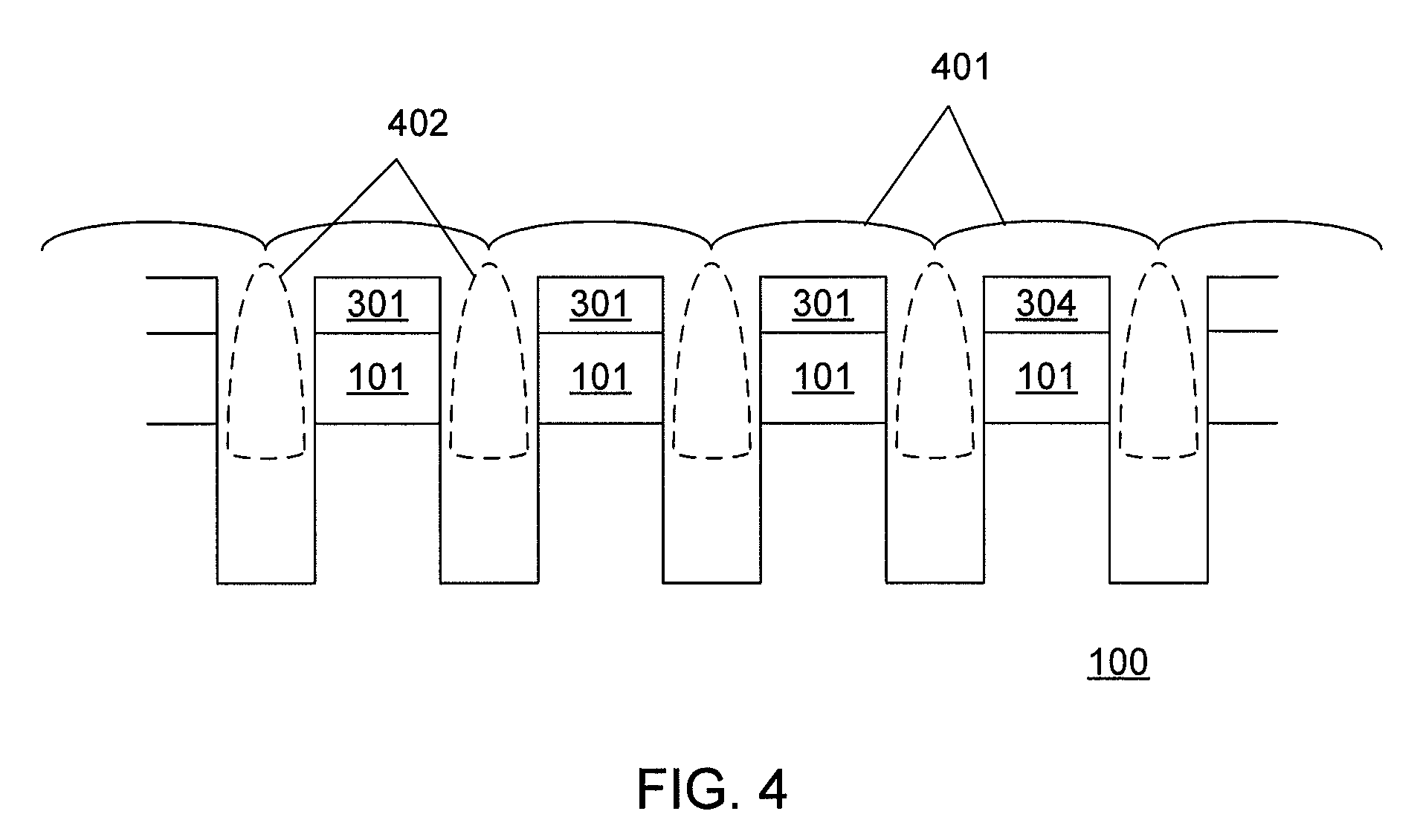
[0017]The invention and the various features and advantageous details are explained more fully with reference to the nonlimiting embodiments that are illustrated in the accompanying drawings and detailed in the following description. Descriptions of well known starting materials, processing techniques, components, and equipment are omitted so as not to unnecessarily obscure the invention in detail. It should be understood, however, that the detailed description and the specific examples, while indicating embodiments of the invention, are given by way of illustration only and not by way of limitation. Various substitutions, modifications, additions, and / or rearrangements within the spirit and / or scope of the underlying inventive concept will become apparent to those skilled in the art from this disclosure.

[0018]The present invention provides systems and methods for reducing the effective dielectric constant of materials used in the fabrication of semiconductor devices. For example, a...


PUM

PropertyMeasurementUnit
dielectric constantaaaaaaaaaa
aspect ratioaaaaaaaaaa
dielectric constantaaaaaaaaaa

Abstract

Systems and methods for controlling the effective dielectric constant of materials used in a semiconductor device are shown and described. In one embodiment, a method comprises providing a semiconductor substrate with a plurality of pillars formed thereon, depositing a first layer of dielectric material over a plurality of pillars, removing a portion of the first layer deposited over the plurality of pillars, and depositing a second layer of dielectric material over the plurality of pillars, where the second layer leaves a plurality of voids between the plurality of pillars.

Description

BACKGROUND OF THE INVENTION[0001]1. Field of the Invention[0002]The present invention relates generally to semiconductor fabrication and, more particularly, to systems and methods for controlling the effective dielectric constant of materials used in a semiconductor device.[0003]2. Description of Related Art[0004]Semiconductor fabrication involves two separate processes. First, devices are created on a wafer surface. Then, those devices are connected to each other using various metal layers in a process called interconnect metallization. One or more layers of dielectric material provide the necessary isolation between metal layers. The dielectric material may be, for example, silicon oxide, silicon nitride, or the like. Once the dielectric is deposited over a metal layer, it is etched in masking step to create vias or plugs, which are openings that expose the underlying metal layer. The vias or plugs are then filled with conductive material.[0005]Although necessary to isolate the va...

Claims


Application Information

Patent Timeline
Patent Type & Authority Patents(United States)
IPC IPC(8): H01L21/4763
CPCH01L21/7682H01L21/76834
Inventor SMITH, GREGORY C.
Owner SEMATECH
Why Eureka
Try Eureka