Package structure of integrated circuit device and manufacturing method thereof

a technology of integrated circuit devices and packaging structures, which is applied in the direction of semiconductor devices, semiconductor/solid-state device details, electrical devices, etc., can solve the problems of inability the thickness of the ceramic substrate cannot be reduced indefinitely, and the thickness cannot be reduced to meet the new requirements of the thin-type package structure, etc., to achieve the effect of improving heat dissipation, reducing the thickness of the package structure, and superior heat conductivity

Inactive Publication Date: 2011-01-04
ADVANCED OPTOELECTRONIC TECH INC
View PDF1 Cites 4 Cited by
  • Summary
  • Abstract
  • Description
  • Claims
  • Application Information

AI Technical Summary

Benefits of technology

[0006]One aspect of the present invention provides a package structure of an integrated circuit device and a manufacturing method thereof. In contrast to conventional ceramic substrates, a copper foil substrate can satisfy the development needs of further reductions in package structure thickness. Moreover, compared with the conventional ceramic substrates, the copper foil substrate improves heat dissipation due to its superior characteristic of heat conductivity.

Problems solved by technology

The ceramic substrates have superior capability to resist heat, but they are inferior in heat conductivity and heat dissipation.
In addition, the ceramic substrates need adequate strength and rigidity so that the thickness of the ceramic substrates cannot be reduced indefinitely.
The thickness of most ceramic substrates ranges from 1 mm to 3 mm, but such thickness cannot meet the new requirements of the thin-type package structure.

Method used


Image

  • Package structure of integrated circuit device and manufacturing method thereof
  • Package structure of integrated circuit device and manufacturing method thereof
  • Package structure of integrated circuit device and manufacturing method thereof

Examples


first embodiment

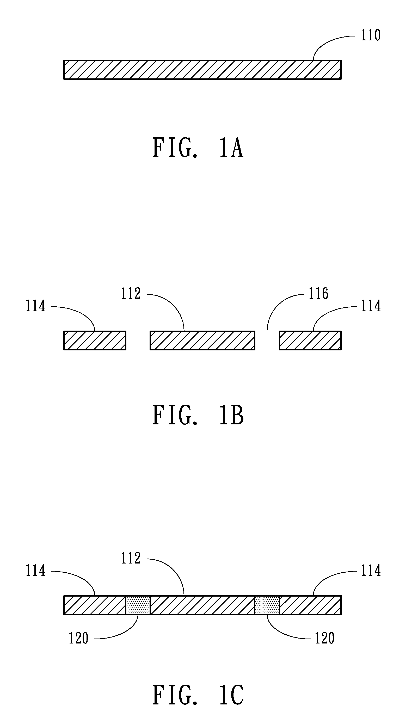
[0019]FIGS. 1A-1C are schematic diagrams illustrating the manufacturing processes of a copper foil substrate in accordance with the present invention. As shown in FIG. 1A, a copper foil substrate 110 with a thickness ranging from 20 μm to 50 μm is provided. Subsequently, as shown in FIG. 1B, a plurality of slots 116 are formed on the copper foil substrate 110 by a drilling process, an etching process and a punching process. Two adjacent conductive areas 114 are isolated from each other through the slots 116, and the conductive areas 114 and the IC bonding area 112 are isolated from each other. Finally, as shown in FIG. 1C, an insulating dielectric material 120 is filled in the slots 116, and the copper foil substrate 100 is completed. The aforesaid insulating dielectric material 120 is selected from the group consisting of SiO, SiN, SiON, TaO, AlO, TiO, AlN, TiN, epoxy resin, silicone and polymer or the combination of elements of the group. The filling of the insulating dielectric m...

second embodiment

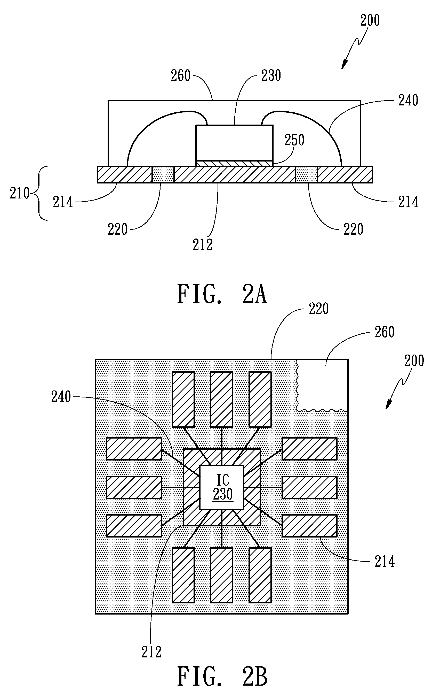
[0020]FIG. 2A is a cross sectional diagram of the package structure of an integrated circuit device in accordance with the present invention. First, a copper foil substrate 210 is provided. The copper foil substrate 210 comprises an IC bonding area 212, a plurality of conductive areas 214 and an insulating dielectric material 220. The insulating dielectric material 220 is between the IC bonding area 212 and the conductive areas 214, and is also between two adjacent conductive areas 214. Subsequently, an integrated circuit device 230 is mounted on the IC bonding area 212 of the copper foil substrate 210 using bonding technology. That is, the integrated circuit device 230 is fixed on the IC bonding area 212 of the copper foil substrate 210 through an adhesive material 250, and is then electrically connected to the plurality of conductive areas 214 of the copper foil substrate 210 through the metal wires 240. Therefore, the copper foil substrate 210 serves as the package carrier of the...

third embodiment

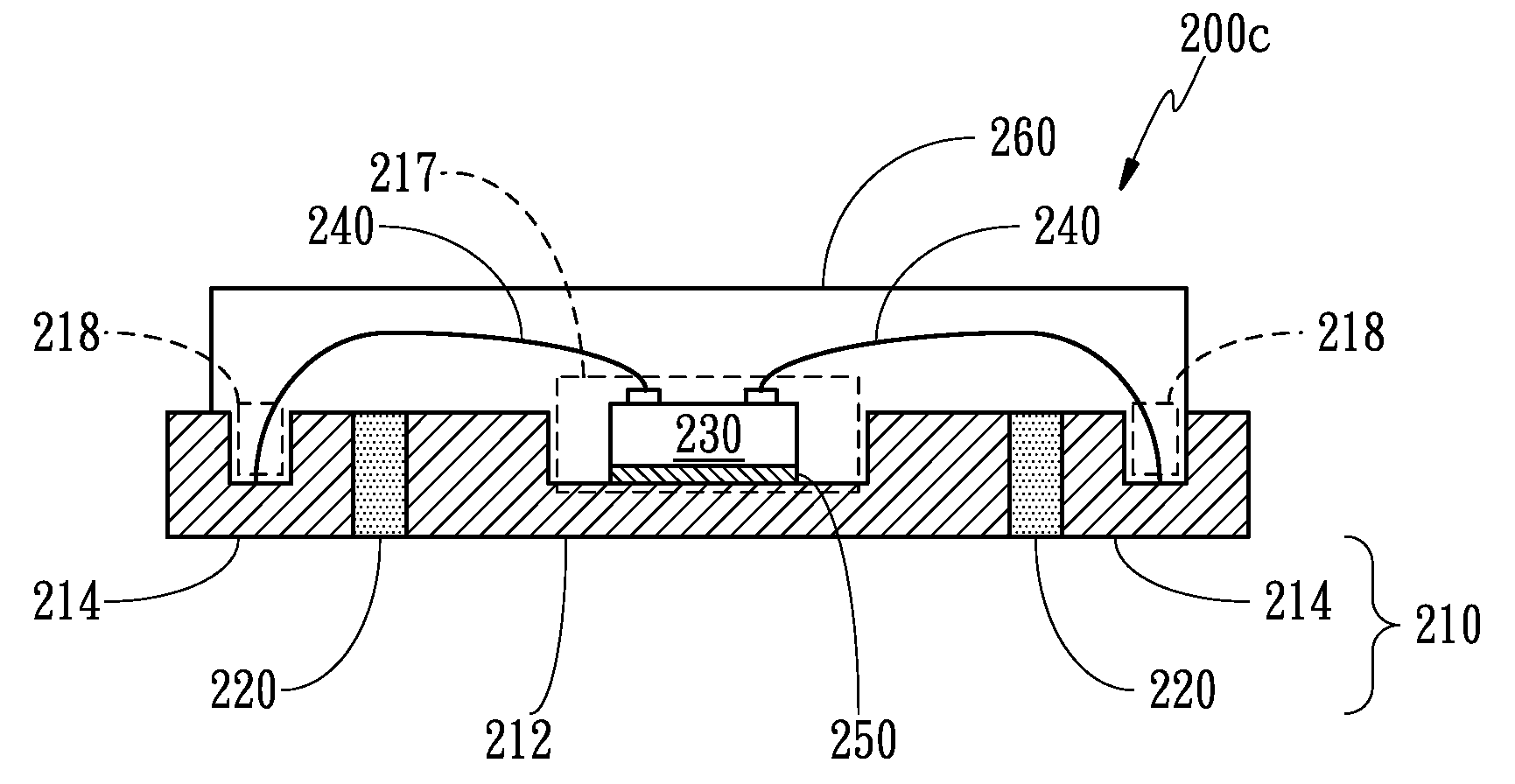
[0025]FIG. 2F is a cross sectional diagram of an IC package structure 200d in accordance with a preferable embodiment of the present invention. Compared with the third embodiment, this embodiment has a different formation method of the die-bonding groove 217 and the wire-bonding grooves 218. A patterned insulating material layer 280 is formed on the copper foil substrate 210. That is, the die-bonding groove 217 and the wire-bonding grooves 218 are formed on the insulating material layer 280 by using a photolithography and etching process. Consequently, not only is the thickness of the package structure reduced, but the metal wires 240 on the conductive areas 214 can also be prevented from shorting due to improperly contacting the IC bonding area 212.

[0026]FIGS. 3A-3D are schematic diagrams illustrating the electroforming processes for forming a die-bonding groove 217 and wire-bonding grooves 218. A copper foil substrate 210 is provided, and a patterned insulating layer 280 is formed...


PUM


Abstract

A package structure of an integrated circuit device comprises a copper foil substrate, an integrated circuit device, a plurality of metal wires and an encapsulation material. The copper foil substrate comprises an IC bonding area, a plurality of conductive areas and an insulating dielectric material. The integrated circuit device is mounted on the surface of the IC bonding area, and is electrically connected to the plurality of conductive areas through the metal wires. The insulating dielectric material is between the IC bonding area and the conductive areas, and is also between two adjacent conductive areas. In addition, the encapsulation material covers the IC bonding area, the conductive areas and the integrated circuit device.

Description

BACKGROUND OF THE INVENTION[0001](A) Field of the Invention[0002]The present invention relates to a package structure of an integrated circuit device and a manufacturing method thereof, and more particularly, to a thin package structure and manufacturing method of an integrated circuit device.[0003](B) Description of the Related Art[0004]Due to rapidly increasing demand for advanced consumer electronic products, and greater requirements for energy-saving and environmentally responsible products, there is a trend toward thinner profiles in current integrated circuit device development. Some conventional integrated circuit packages utilize ceramic substrates. The ceramic substrates have superior capability to resist heat, but they are inferior in heat conductivity and heat dissipation. In addition, the ceramic substrates need adequate strength and rigidity so that the thickness of the ceramic substrates cannot be reduced indefinitely. The thickness of most ceramic substrates ranges fr...

Claims


Application Information

Patent Timeline
Patent Type & Authority Patents(United States)
IPC IPC(8): H01L21/98
CPCH01L23/3107H01L23/49861H01L2224/32257H01L2224/16245H01L2224/32245H01L2224/48247H01L2224/49171H01L2224/73265H01L2924/00H01L2924/01322H01L2224/05573H01L2224/05568H01L2924/00014H01L2224/05599H01L2924/00012
Inventor CHAN, SHIH HSIUNGLIN, SHEN BOCHEN, PIN CHUAN
Owner ADVANCED OPTOELECTRONIC TECH INC
Why Eureka
Try Eureka