Electro-optical device and electronic apparatus

a technology of optical elements and electronic devices, applied in static indicating devices, electroluminescent light sources, instruments, etc., can solve the problems of non-uniform gray-scale levels of optical elements, inability to achieve realistic solutions, and low resolution pixels, and achieve simplified wiring arrangements

Inactive Publication Date: 2011-01-11
SEIKO EPSON CORP
View PDF16 Cites 4 Cited by
  • Summary
  • Abstract
  • Description
  • Claims
  • Application Information

AI Technical Summary

Benefits of technology

[0010]An advantage of some aspects of the invention is that fluctuation in electric potential of the gate of a driving transistor is suppressed and the wiring arrangement is simplified.
[0018]In this configuration, as the driving transistor is diode-connected through the first switching element, a driving current that is not dependent on a threshold voltage of the driving transistor is generated. In addition, as the second switching element turns on (conduction state), the gate of the driving transistor is set to an electric potential corresponding to the data electric potential, while, on the other hand, as the second switching element turns off (non-conduction state), the third switching element turns on, so the first electrode of the capacitive element is maintained at a constant electric potential. Thus, it is possible to prevent fluctuation in electric potential of the gate of the driving transistor while avoiding an increase in capacitance provided on the unit circuit.
[0019]Furthermore, according to the second aspect of the invention, each of the power feed lines is arranged so as to Intersect with the scanning lines. For example, when the scanning lines are arranged in rows, the power feed lines may be arranged in columns. When the first switching element and the fourth switching element are simultaneously brought into conduction states, threshold compensation of the driving transistor may be executed. The electric current of the diode-connected driving transistor then flows into the power feed line. If the power feed lines are arranged in rows in the same directions as the scanning lines, electric current simultaneously flows into the power feed line from the plurality of unit circuits that are arranged in the same row. For this reason, the width of the power feed line needs to be larger so that it can allow a large electric current to flow therethrough. In contrast, when the power feed line is arranged in a direction that intersects with the scanning lines, the magnitude of electric current that flows thereinto is an amount of a single unit circuit, so that it is possible to reduce the width of the power feed line. Hence, the wiring arrangement may be simplified to achieve high-integration.
[0020]A specific embodiment according to the second aspect of the invention may further include a plurality of power supply lines, each of which supplies the driving transistor of each of the plurality of unit circuits with power supply voltage, wherein the power supply lines intersect with the power feed lines at intersections, and a holding capacitor that is formed at each of the intersections. In this case, it is possible to further stabilize the electric potential of the power feed line by the holding capacitor.
[0021]In a specific embodiment according to the second aspect of the invention, in each of the plurality of unit circuits, the second switching element and the third switching element may be transistors of different conductivity types, and a common scanning signal may be supplied to the gate of the second switching element and the gate of the third switching element. According to this aspect, because a wiring for controlling the second switching element and a wiring for controlling the third switching element may be shared, it is possible to simplify the wiring arrangement.

Problems solved by technology

However, this configuration is disadvantageous in that electro-optical elements have nonuniform gray-scale levels due to individual differences in characteristics (particularly, in threshold voltage) among driving transistors.
However, in this case, because there is a problem that the scale of the pixel circuit P0 increases due to the increase in capacitance, it cannot be a realistic solution under the present circumstances where high-resolution pixels are highly required.

Method used


Image

  • Electro-optical device and electronic apparatus
  • Electro-optical device and electronic apparatus
  • Electro-optical device and electronic apparatus

Examples


first alternative embodiment

(1) First Alternative Embodiment

[0070]In the above described embodiments, the configuration in which the transistor Tr2 and the transistor Tr3 are transistors of different conductivity types is illustrated; however, the configuration for activating the transistor Tr2 and the transistor Tr3 in a complimentary manner is not limited to it. For example, as shown in FIG. 11, the transistor Tr2 and the transistor Tr3 may be transistors of the same conductive types (n-channel type) with respect to each other. With this configuration, the gate of the transistor Tr2 is connected to a first scanning line 121a, and the gate of the transistor Tr3 is connected to a second scanning line 121b. Then, the first scanning line 121a is supplied with a first scanning signal GWRT[i] having the same waveform as the scanning signal GWRT[i] shouts on FIG. 4, and the second scanning line 121b is supplied with a second scanning signal GWRTb[i] having the inverted logic level with respect to the first scanning...

second alternative embodiment

(2) Second Alternative Embodiment

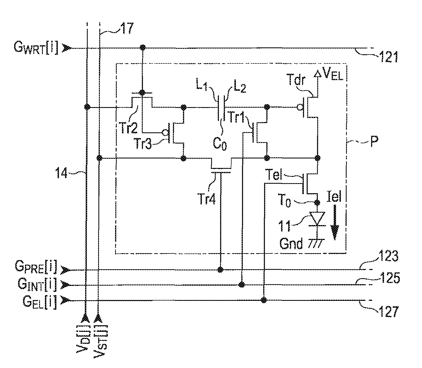
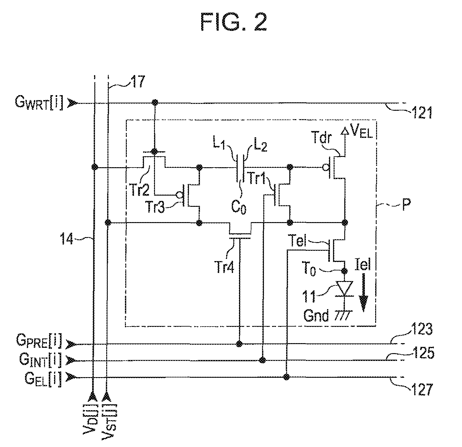
[0071]The transistor Tr4 and / or the light emission control transistor Tel are omitted where appropriate. FIG. 12 is a circuit diagram snowing a configuration of the pixel circuit P in which the transistor Tr4 and the light emission control transistor Tel shown in FIG. 2 are omitted. With this configuration, during the initialization period PINT, the scanning signal GWRT[i] attains a low level, and the initialization signal GINT[i] attains a high level. Thus, the first electrode L1 is maintained at the electric potential VST by turning on the transistor Tr3, the gate of the driving transistor Tdr that is diode-connected through the transistor Tr1 converges on the electric potential VG(=VEL−Vth) corresponding to the threshold voltage Vth.

[0072]During the subsequent writing period PWRT, the initialization signal GINT[i], which is in a low level, turns off the transistor Tr1. Furthermore, as the scanning signal GWRT[i] is changed to a high level, the tra...

third alternative embodiment

(3) Third Alternative Embodiment

[0074]Conductive types of the transistors that form the pixel circuit P may be changed where appropriate. For example, the driving transistor Tdr shown in FIG. 2 may be of an n-channel type. In this case, the electric potential VST supplied to the power feed line 17 is set to an electric potential that turns on the driving transistor Tdr when the gate of the driving transistor Tdr is supplied with the electric potential VST. Note that, when the driving transistor Tdr is of an n-channel type, the transistor Td1 is connected between the gate of the driving transistor Tdr and the power supply line (electric potential VEL). In addition, the OLED element is just one of examples of the electro-optical element 11. For example, in place of the OLED element, various light-emitting elements, such as an inorganic EL element or an LED (Light Emitting Diode) element, may be employed as an electro-optical element according to the aspects of the invention. The elect...


PUM


Abstract

An electro-optical device includes a plurality of data lines, a plurality of scanning lines, a plurality of unit circuits that are provided in correspondence with intersections of the data lines and the scanning lines. Each of the data lines is supplied with a data voltage in accordance with a gray-scale level. Each of the scanning lines is supplied with a scanning signal that specifies a writing period during which the data voltage is being written into the corresponding unit circuits. Each of the plurality of unit circuits includes a driving transistor, an electro-optical element, a capacitive element, a power feed line, a first switching element and a second switching element. The driving transistor generates a driving current in accordance with an electric potential of a gate thereof. The electro-optical element generates light with a gray-scale level in accordance with the driving current that is generated by the driving transistor. The capacitive element has a first electrode and a second electrode that is connected to the gate of the driving transistor. The power feed line is supplied with a constant electric potential and is, during an initialization period that is different from the writing period, electrically connected to the second electrode. The first switching element conducts the gate of the transistor with the drain thereof at least during the initialization period. The second switching element switches between conduction and non-conduction between the data line and the first electrode on the basis of the scanning signal. The power feed line is arranged in a direction that intersects with the scanning lines.

Description

BACKGROUND[0001]The entire disclosure of Japanese Patent application No. 2006-247654, filed Sep. 13, 2006 is expressly incorporated by reference herein.[0002]1. Technical Field[0003]The present invention relates to a technology that controls the operations of various electro-optical elements, such as light-emitting devices made of organic EL (ElectroLuminescent) material.[0004]2. Related Art[0005]In electro--optical elements made of organic EL material, gray-scale level (typically, luminance) is changed in accordance with an electric current supplied thereto. A configuration for controlling the electric current (hereinafter, referred to as “driving current”) by means of a transistor (hereinafter, referred to as “driving transistor”) has been proposed. However, this configuration is disadvantageous in that electro-optical elements have nonuniform gray-scale levels due to individual differences in characteristics (particularly, in threshold voltage) among driving transistors. A config...

Claims


Application Information

Patent Timeline
Patent Type & Authority Patents(United States)
IPC IPC(8): G09G3/30H05B44/00
CPCG09G3/3233G09G2300/0819G09G2320/045G09G2320/0209G09G2300/0861G09G3/30G09G3/20G09G3/32
Inventor KANDA, EIJI
Owner SEIKO EPSON CORP
Why Eureka
Try Eureka