Method for manufacturing semiconductor light-emitting device

a light-emitting device and semiconductor technology, applied in semiconductor lasers, lasers, laser details, etc., can solve the problems of reducing direct-modulation bandwidth, increasing threshold current and power consumption, and complicated succeeding steps, so as to reduce light absorption and reduce the effect of reliability degradation, avoiding degradation of reliability

Active Publication Date: 2011-01-18
SONY CORP
View PDF44 Cites 4 Cited by
  • Summary
  • Abstract
  • Description
  • Claims
  • Application Information

AI Technical Summary

Benefits of technology

[0011]However, in Japanese Unexamined Patent Publication No. 2004-179640, other measures are necessary for suppressing light absorption of the In-containing layer itself and avoiding degradation of reliability. In Japanese Unexamined Patent Publication No. 2003-158340, there are issues that a threshold current and power consumption increase, a direct-modulation bandwidth decreases, and the like. Further, in Japanese Unexamined Patent Publication Nos. 2004-179640 and 2003-158340, the growth of the damage starting from the oxidation front may not be suppressed and the deformation caused by the volume shrinkage during the oxidation in the layers other than the current confinement layer 115 in the vertical cavity structure may not be suppressed either.
[0014]In view of the foregoing, it is desirable to provide a method of manufacturing a semiconductor light-emitting device having a mesa with a height no higher than necessary, and capable of suppressing a growth of damage starting from an oxidation front and deformation caused by a volume shrinkage during oxidation in layers except a current confinement layer in a vertical cavity structure.

Problems solved by technology

In Japanese Unexamined Patent Publication No. 2003-158340, there are issues that a threshold current and power consumption increase, a direct-modulation bandwidth decreases, and the like.
Thus, the mesa 118 becomes higher than necessary, and this makes succeeding steps complicated.

Method used


Image

  • Method for manufacturing semiconductor light-emitting device
  • Method for manufacturing semiconductor light-emitting device
  • Method for manufacturing semiconductor light-emitting device

Examples


Embodiment Construction

[0042]Preferred embodiments of the present invention will be described in detail with reference to the accompanying drawings.

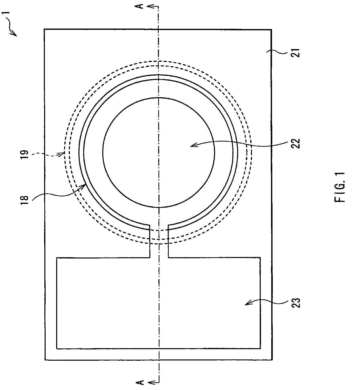
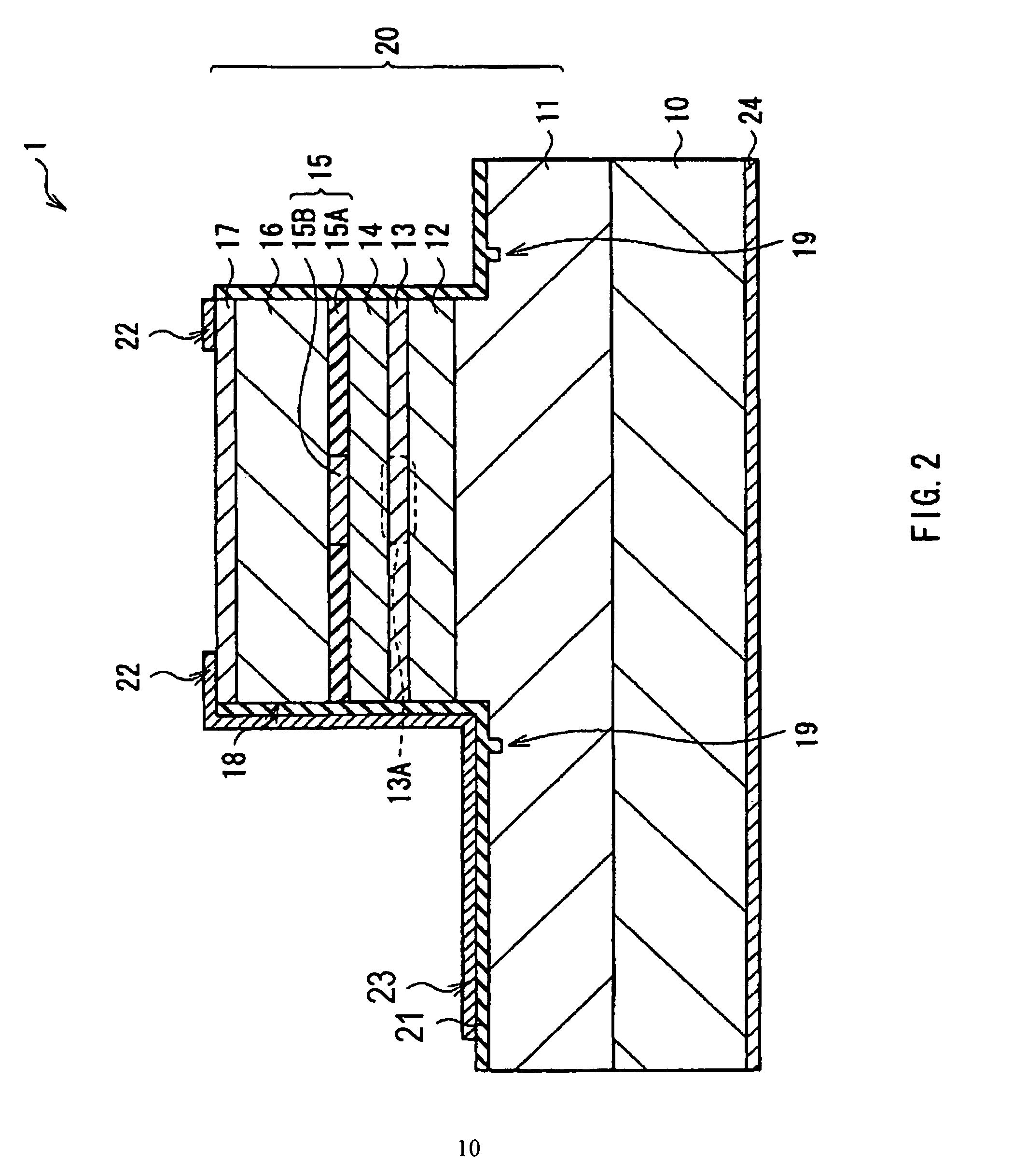
[0043]FIG. 1 illustrates a top surface view of a surface-emitting laser diode 1 according to an embodiment of the present invention. FIG. 2 illustrates a cross-sectional configuration as viewed from the direction of an arrow A-A of FIG. 1.

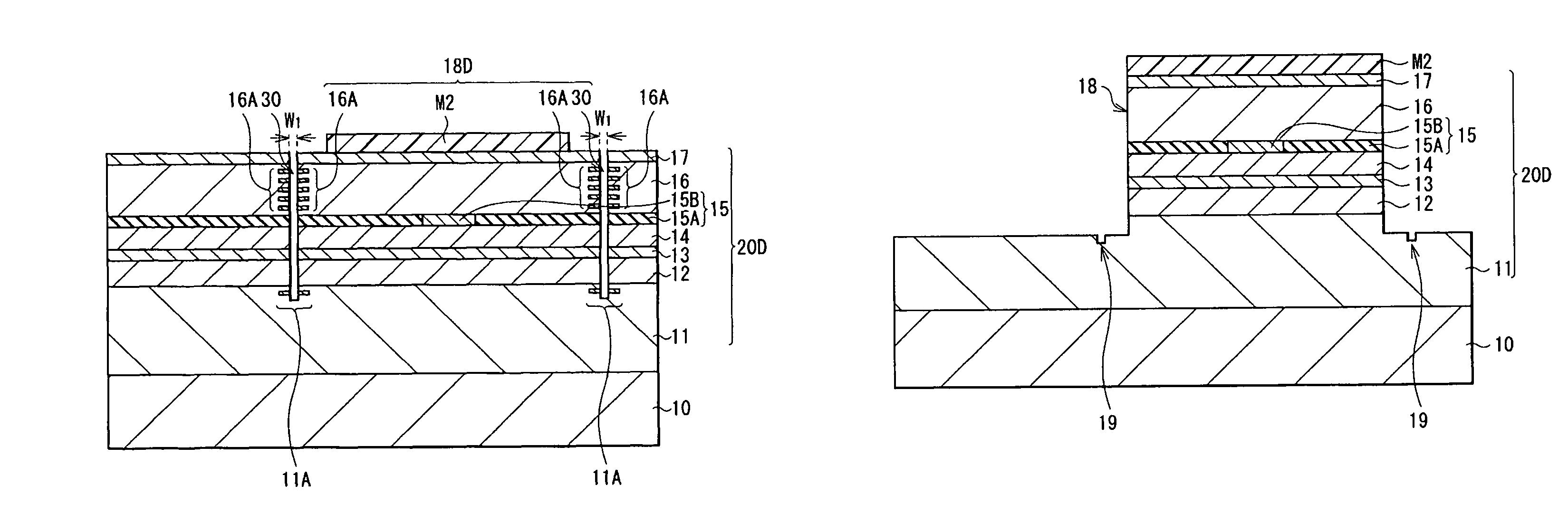
[0044]The laser diode 1 according to the embodiment of the present invention includes a semiconductor stacked structure 20 (a vertical cavity structure) on a surface of a substrate 10. The semiconductor stacked structure 20 is configured by stacking a lower DBR layer 11, a lower spacer layer 12, an active layer 13, an upper spacer layer 14, a current confinement layer 15, an upper DBR layer 16, and a contact layer 17 in this order from the substrate 10 side. A columnar mesa 18 is formed in an upper part of the semiconductor stacked structure 20, specifically, in a part of the lower DBR layer 11, the lower spacer layer 12, the...


PUM


Abstract

A method of manufacturing a semiconductor light-emitting device includes steps of forming a vertical cavity structure including a layer to be oxidized on a semiconductor substrate, and then forming a circular groove having a depth which penetrates at least the layer to be oxidized from an upper surface of the vertical cavity structure, thereby forming a columnar mesa whose side face is surrounded by the groove, oxidizing the layer to be oxidized from the side face of the mesa, thereby forming a current confinement layer, and forming a mask layer covering at least a central region of the upper surface of the mesa and exposing at least an edge of the upper surface and the side face of the mesa to an external, and then etching at least the edge of the upper surface and the side face of the mesa by using the mask layer as a mask.

Description

CROSS REFERENCES TO RELATED APPLICATIONS[0001]The present invention contains subject matter related to Japanese Patent Application JP 2007-267871 filed in the Japanese Patent Office on Oct. 15, 2007, the entire contents of which being incorporated herein by reference.BACKGROUND OF THE INVENTION[0002]1. Field of the Invention[0003]The present invention relates to a method of manufacturing a semiconductor light-emitting device including a vertical cavity structure.[0004]2. Description of the Related Art[0005]A surface-emitting laser diode differs from an edge-emitting laser diode of the related art in that the surface-emitting laser diode emits a light in a direction orthogonal to a substrate, and allows multiple devices to be arranged in a two-dimensional array on the same substrate. Thus, the surface-emitting laser diode has attracted attention in recent years as a light source used for a digital copying machine and a printer.[0006]As shown in FIG. 16, for example, this type of surf...

Claims


Application Information

Patent Timeline
Patent Type & Authority Patents(United States)
IPC IPC(8): H01L21/00H01S5/22
CPCH01S5/18311H01S5/18358H01S5/2086
Inventor MASUI, YUJIARAKIDA, TAKAHIROYAMAUCHI, YOSHINORIKODA, RINTAROOKI, TOMOYUKI
Owner SONY CORP
Why Eureka
Try Eureka