
Look-ahead built-in self tests

Inactive Publication Date: 2011-01-25
INTEGRATED DEVICE TECH INC
View PDF9 Cites 15 Cited by
  • Summary
  • Abstract
  • Description
  • Claims
  • Application Information

AI Technical Summary

Benefits of technology

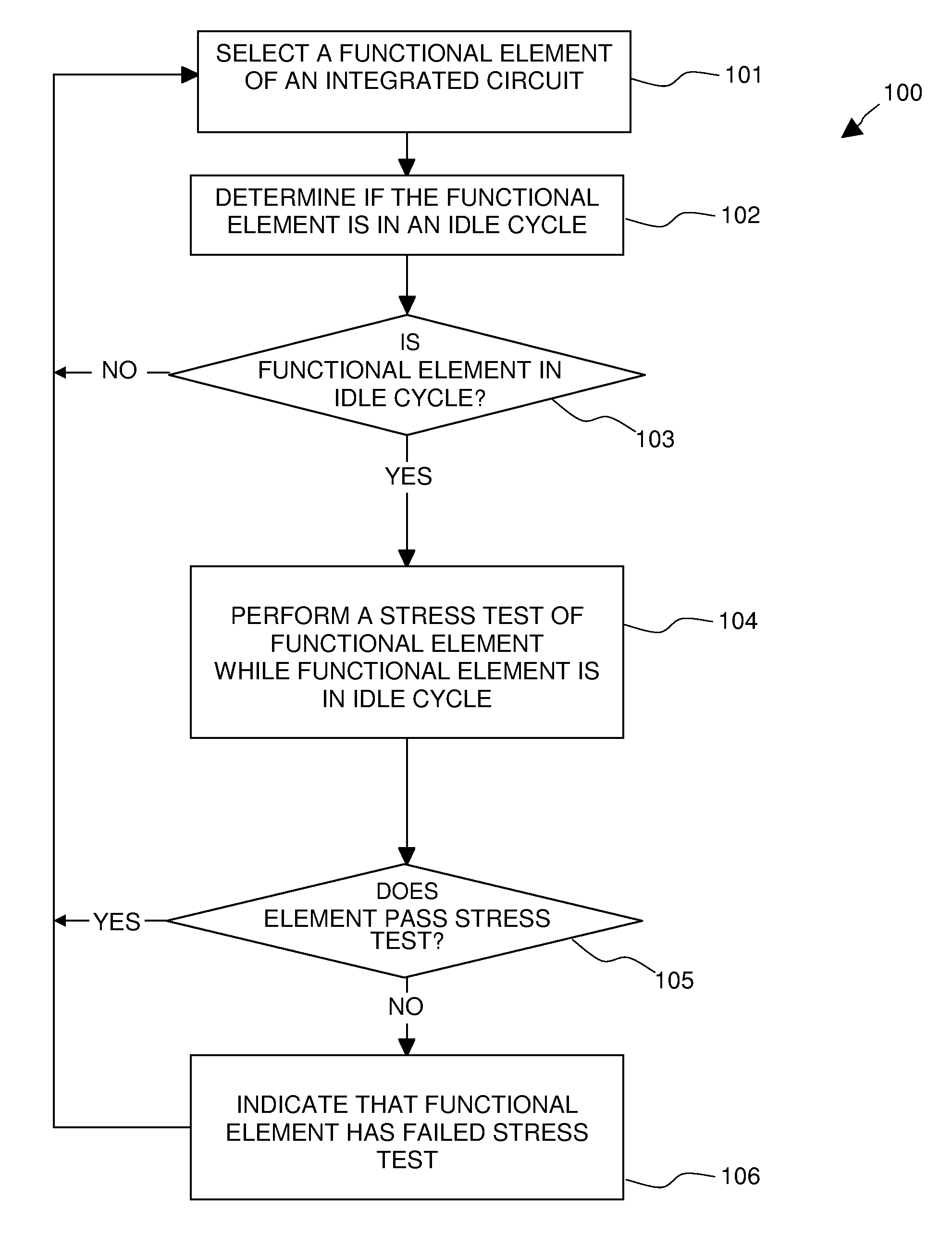
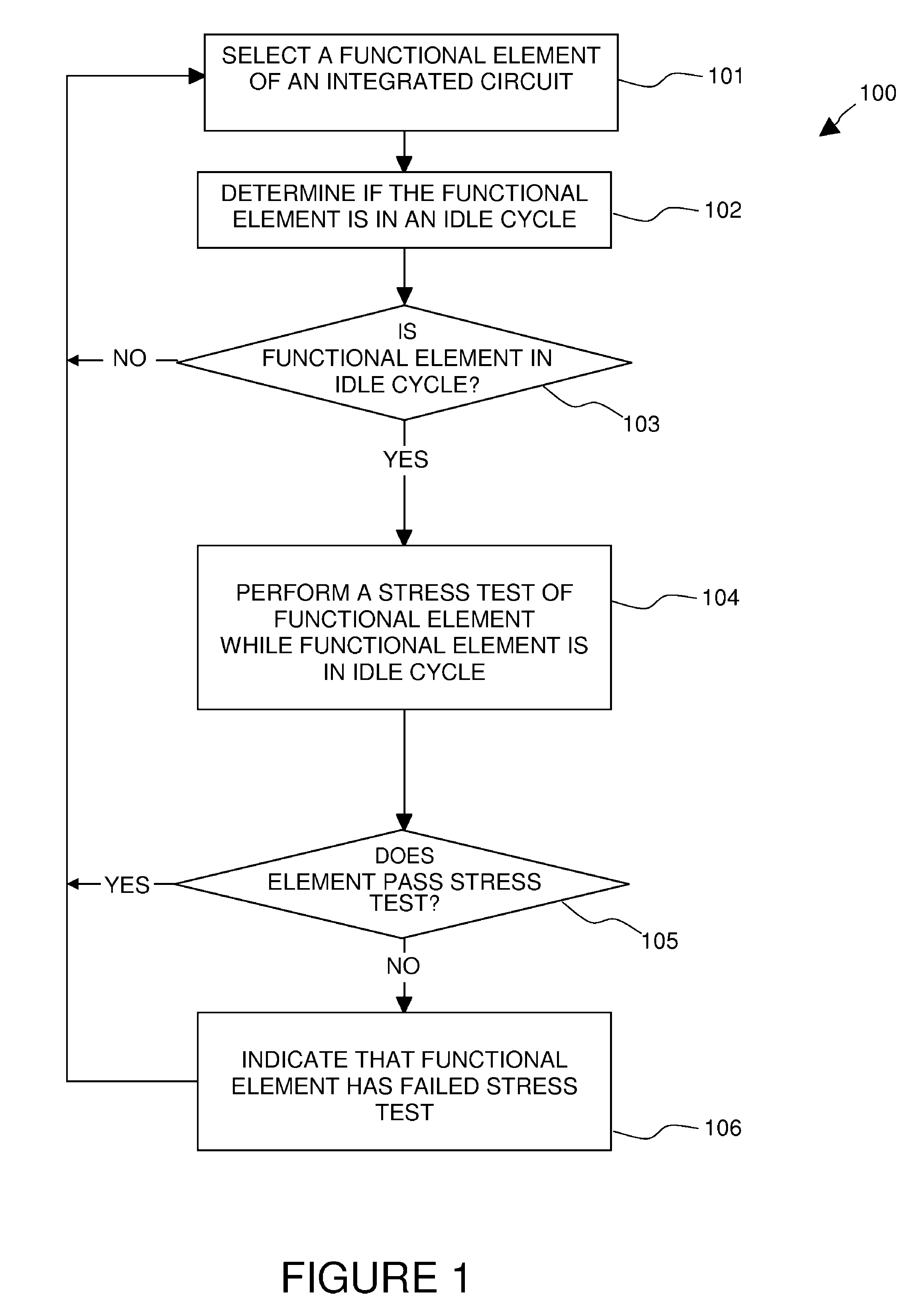
[0009]In the present embodiment the stress test is performed in the background, during continuous operation of the integrated circuit device, such that normal operation of the integrated circuit device is not interrupted. Thereby, the method and apparatus of the present invention allows for failure prediction in a device before it happens, allowing for planned outages or workarounds and avoiding system downtime for unplanned repairs and the extra cost of complete redundant systems and boards.

Problems solved by technology

As electronic devices are implemented in ever smaller geometries, there is an increasing chance of failure over the life of a device due to changes resulting from changes in the materials.
Several phenomena can reduce the reliability margin of a device.
Failures resulting from these phenomena are often only discovered later in the life of a system, long after manufacture and initial testing.
Even very complex devices can survive a myriad of in-production and post-production tests but still harbor potential failures that aren't discovered until late in the device's life.
Such failures can be detected after installation but usually require that the appliance or system in which a device operates is taken out of operation for testing.
However, the locating and replacing do not take place until the system fails, incurring the cost and inconvenience of a system shutdown of the entire system or a board.
The cost can also be in lost operating revenue and / or redundant functional boards and systems as back up for failures.
However, predicting failure is not easy.

Method used


Image

  • Look-ahead built-in self tests
  • Look-ahead built-in self tests
  • Look-ahead built-in self tests

Examples


Embodiment Construction

[0017]Reference will now be made in detail to the preferred embodiments of the invention, examples of which are illustrated in the accompanying drawings. While the invention will be described in conjunction with the preferred embodiments, it will be understood that they are not intended to limit the invention to these embodiments. On the contrary, the invention is intended to cover alternatives, modifications and equivalents, which may be included within the spirit and scope of the invention as defined by the appended claims. Furthermore, in the following detailed description of the present invention, numerous specific details are set forth in order to provide a thorough understanding of the present invention. However, it will be obvious to one of ordinary skill in the art that the present invention may be practiced without these specific details. In other instances, well-known methods, procedures, components, and circuits will not be described in detail so as to avoid obscuring asp...


PUM


Abstract

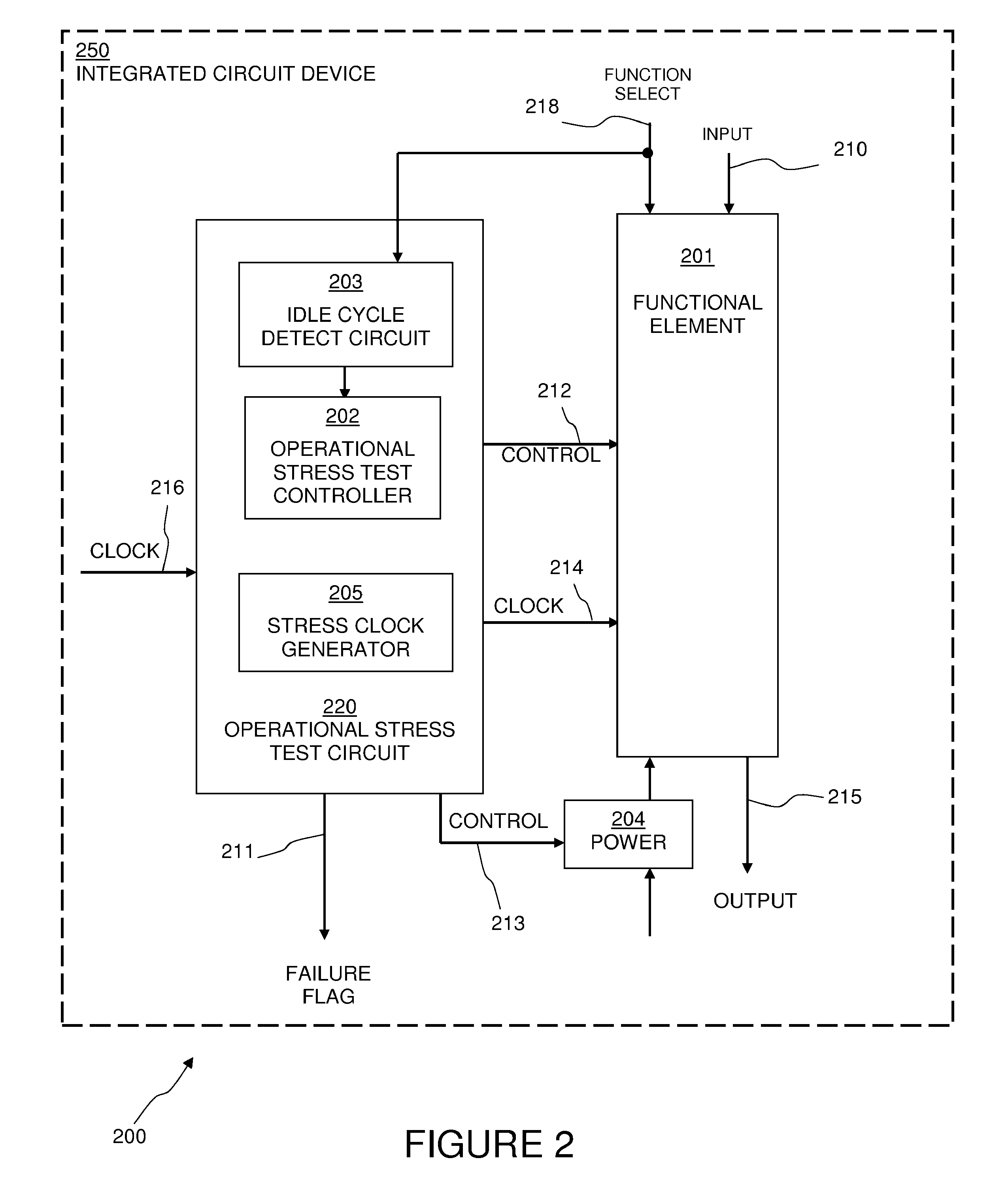
A method and apparatus are disclosed for predicting the failure of a functional element of an integrated circuit during operation. The method includes determining whether the functional element of the integrated circuit device is in an idle cycle, performing a stress test of the functional element while the functional element is in the idle cycle, and indicating that the functional element, if it fails the stress test, is a potential future failing element. The stress test can include simultaneously providing a margining test voltage and a stress clock signal to the functional element. The stress test is performed in the background, during continuous operation of the integrated circuit device, such that normal operation of the integrated circuit device is not interrupted. Thereby, the method and apparatus of the present invention allows for failure prediction in a device before it happens, allowing for planned outages or workarounds and avoiding system downtime for unplanned repairs.

Description

CROSS-REFERENCE TO RELATED APPLICATIONS[0001]The present application claims benefit of U.S. Provisional Patent Application Ser. No. 60 / 908,934, filed Mar. 29, 2007, entitled “LOOK-AHEAD BUILT-IN SELF TESTS.”BACKGROUND OF THE INVENTION[0002]Modern complex electronic devices are rigorously tested during and after production. As electronic devices are implemented in ever smaller geometries, there is an increasing chance of failure over the life of a device due to changes resulting from changes in the materials. One well-known change resulting from device-material-drift is negative bias temperature instability (NBTI). Another is the “hot carrier effect”. Both can change device behavior during operations. Resistances of conductors in a device can also change over time due to electro-migration.[0003]Several phenomena can reduce the reliability margin of a device. One is the total number of elements (e.g., transistors, interconnects, contacts, vias, etc.) in a device. If the probability of...

Claims


Application Information

Patent Timeline
IPC IPC(8): G01R31/3187G01R31/40
CPCG01R31/3016G01R31/318519
Inventor MILLER, MICHAELLIEN, CHUEN-DER
Owner INTEGRATED DEVICE TECH INC
Learn More