

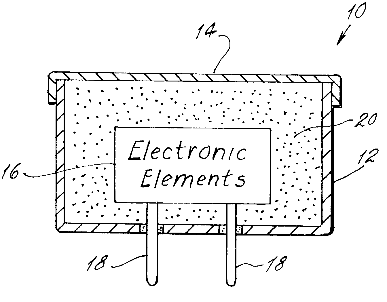
Potting material for electronic components
- Summary
- Abstract
- Description
- Claims
- Application Information
AI Technical Summary
Benefits of technology
Problems solved by technology
Method used
Image

Examples
Embodiment Construction
[0013]For a better understanding of the present invention, together with other and further objects, advantages and capabilities thereof, reference is made to the following disclosure and appended claims in conjunction with the above-described drawings.
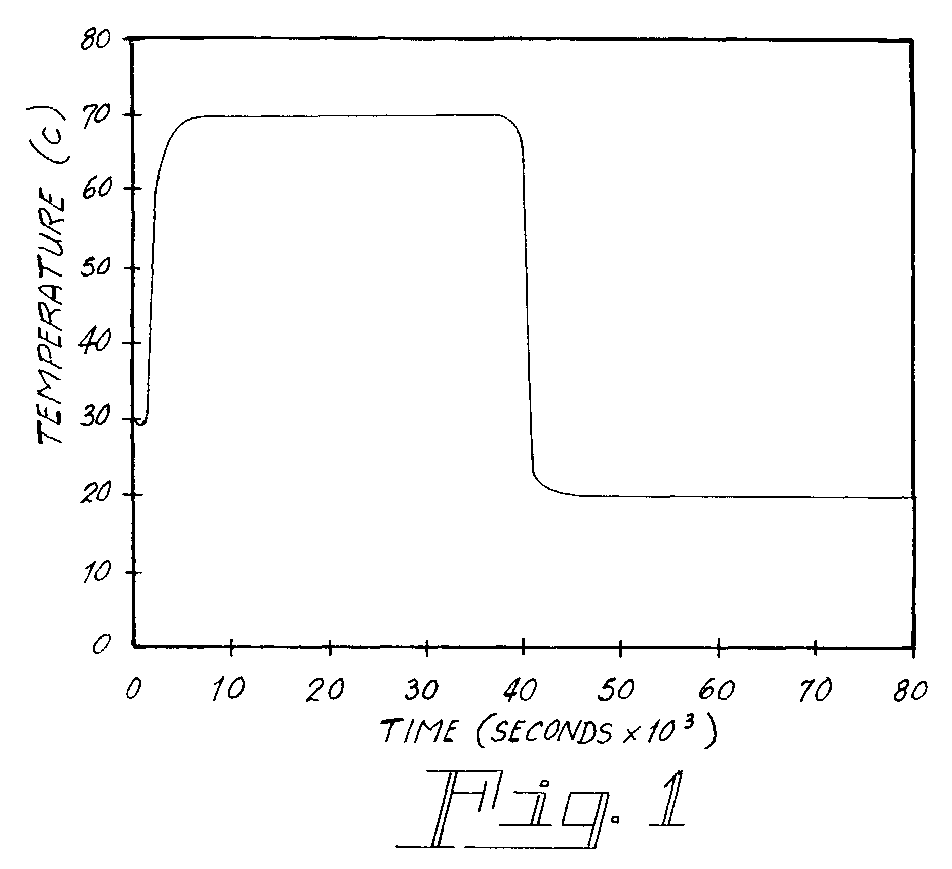
[0014]Referring now to the drawings with greater particularity, there is shown in FIG. 1 a graph of a temperature cycle used for testing potted electronic elements. This standard temperature cycle involves heating to 70° C. for 12 hours, followed by 10 hours at 20° C.
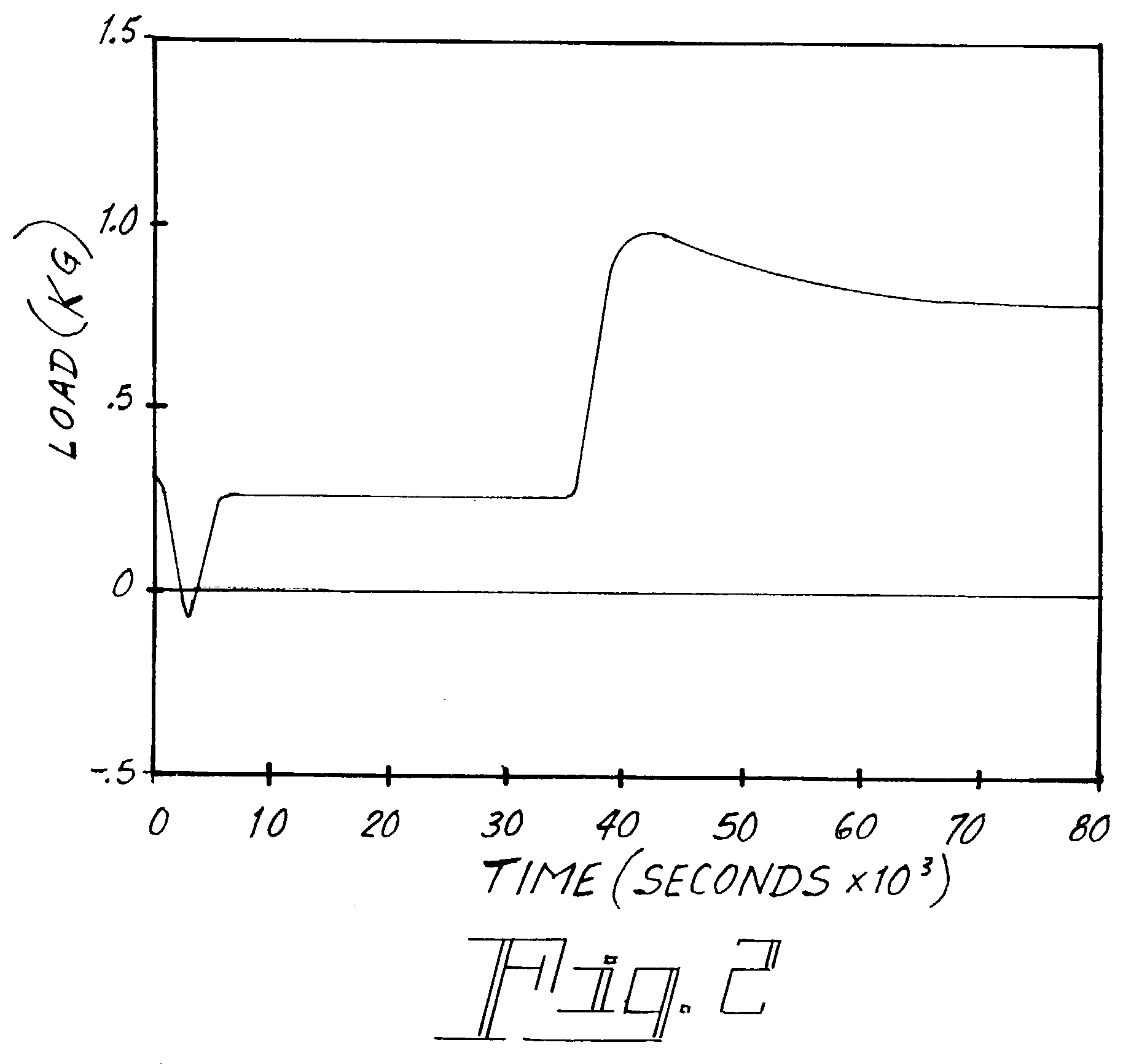
[0015]FIG. 2 is a plot of the forces applied during this temperature cycle by a prior art potting compound comprised of an asphalt and sand mixture. As will be seen from the plot the peak force applied by this prior art compound is approximately 1 Kg.
[0016]FIG. 3 illustrates the difference when a potting compound with a force attenuator added is used. With the force attenuator the maximum force applied to the components is approximately 0.4 Kg during the above-described st...
PUM
| Property | Measurement | Unit |
|---|---|---|
| Force | aaaaa | aaaaa |
Abstract
Description
Claims
Application Information