Operational amplifier and method of driving liquid crystal display
a technology of liquid crystal display and operation amplifier, which is applied in the direction of static indicating devices, instruments, phase splitters, etc., can solve problems such as the ability to cancel, and achieve the effect of increasing the circuit area
- Summary
- Abstract
- Description
- Claims
- Application Information
AI Technical Summary
Benefits of technology
Problems solved by technology
Method used
Image

Examples
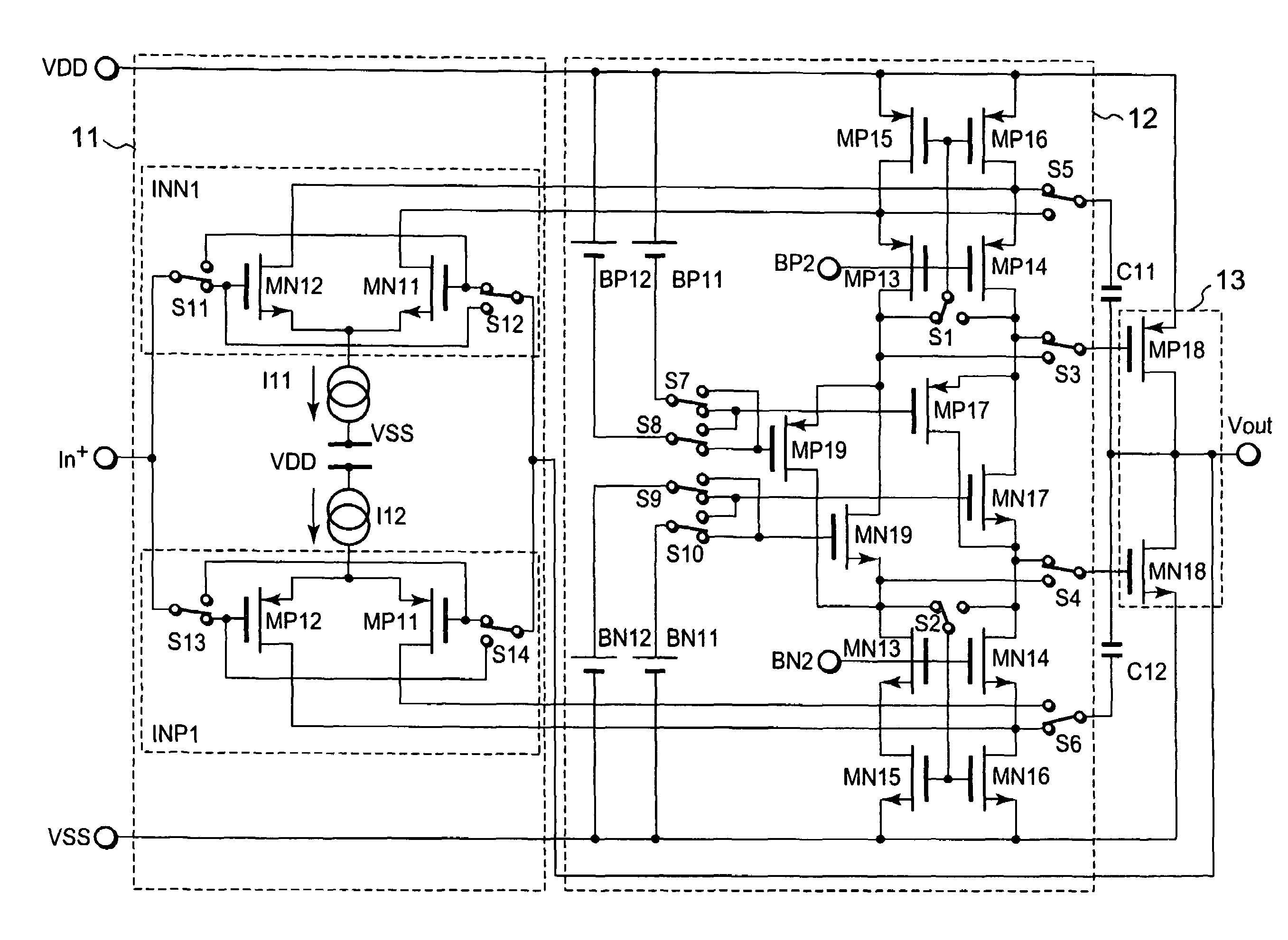
embodiment 2
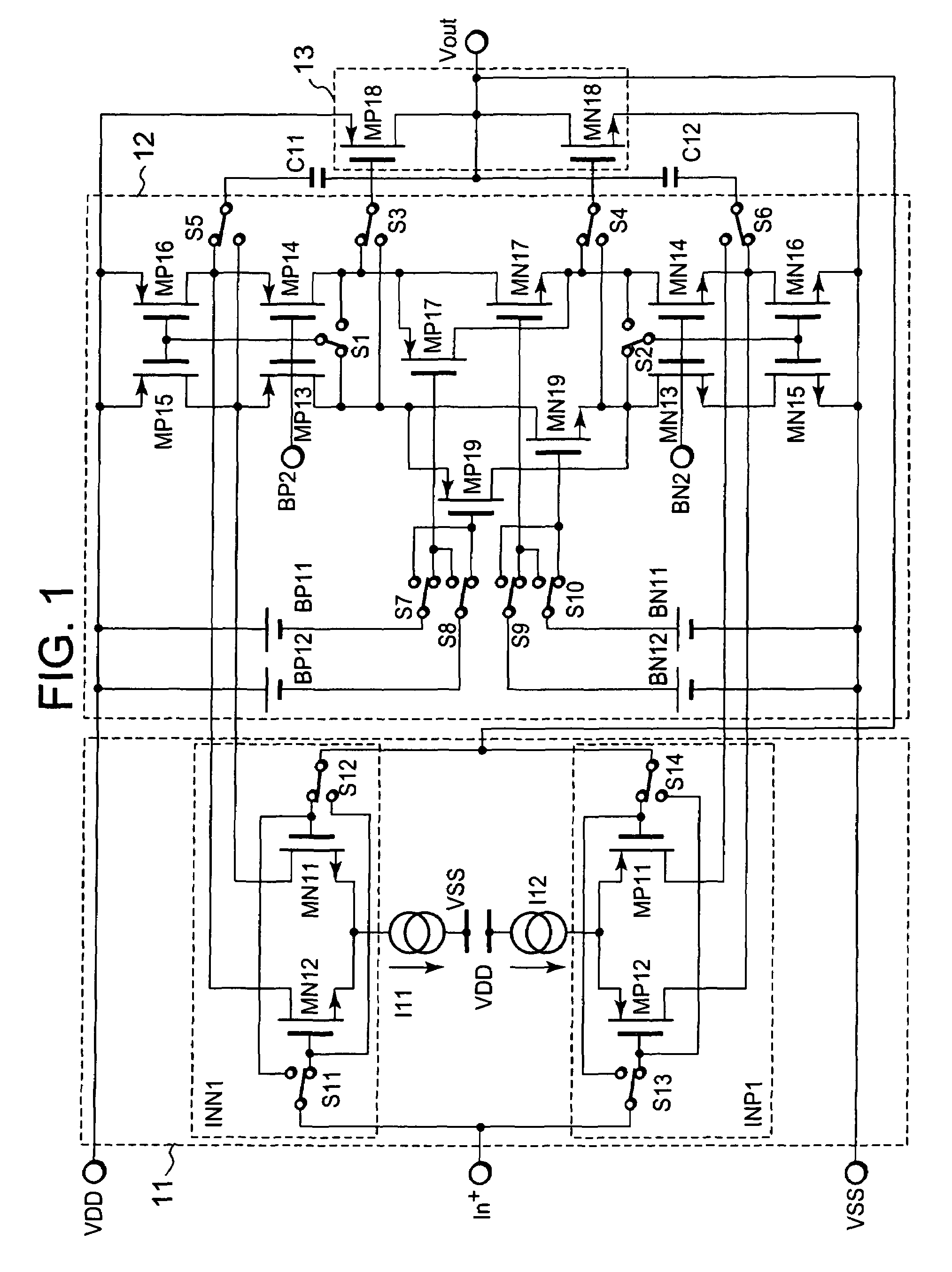
[0064]FIG. 2 is a circuit diagram illustrating an operational amplifier of a second embodiment of the present invention. Like portions in FIG. 2 to the portions described in FIG. 1 are designated by like symbols and their description will be omitted. The circuit diagram shown in FIG. 2 illustrates an example in which a switch is eliminated from the circuit shown in FIG. 1.
[0065]Referring to FIG. 2, a node at which a source of a P channel MOS transistor MP27 and a drain of an N channel MOS transistor MN27 are commonly connected to each other is disconnected from the drain of the P channel MOS transistor MP14 shown in FIG. 1 and connected to a common terminal of a switch S3. Further, a node at which a drain of the P channel MOS transistor MP27 and a source of the N channel MOS transistor MN27 are commonly connected to each other is disconnected from the drain of the N channel MOS transistor MN14 shown in FIG. 1 and connected to a common terminal of a switch S4. Due to this connection,...
embodiment 3
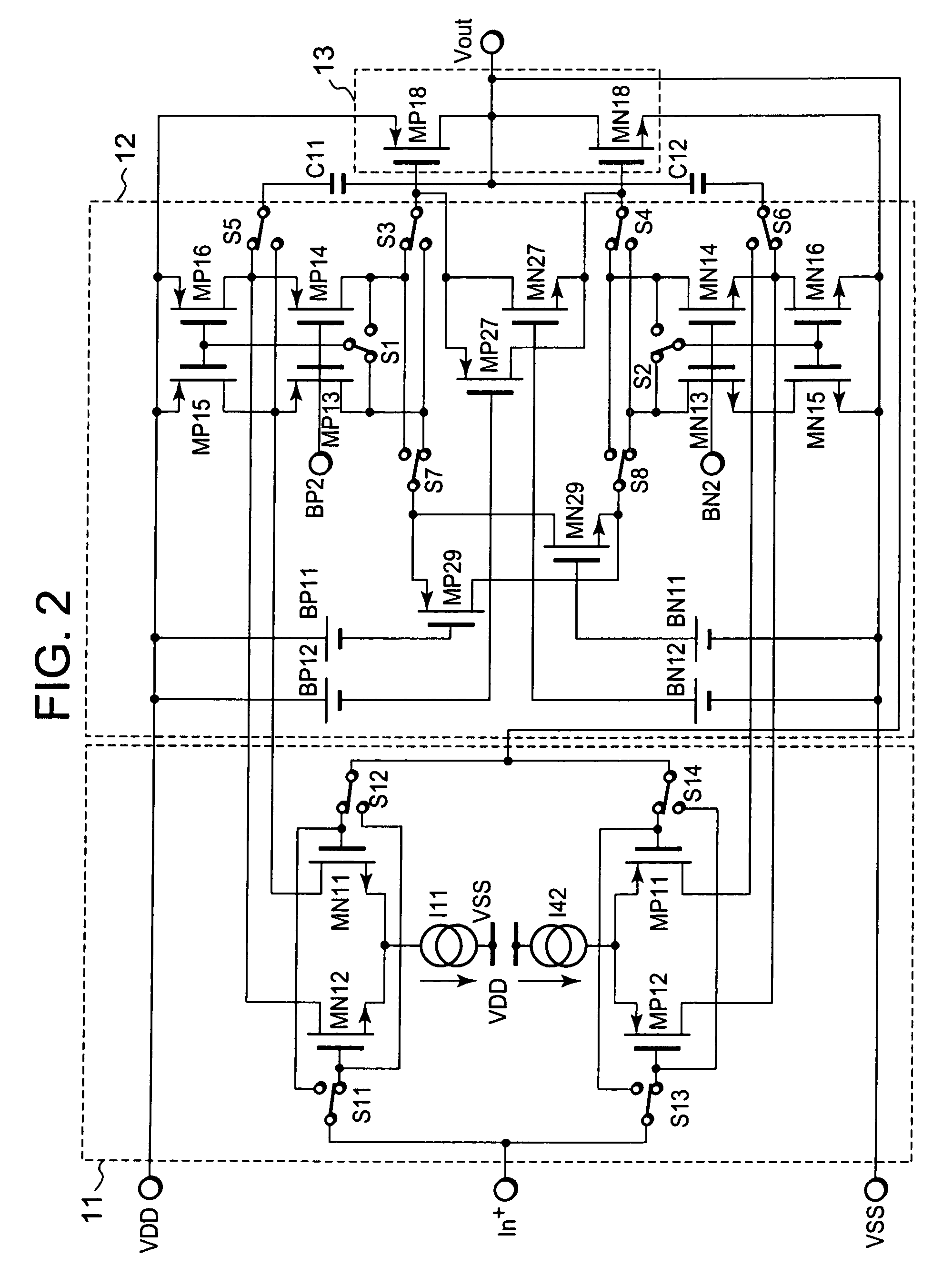
[0069]FIG. 3 is a circuit diagram illustrating an operational amplifier of a third embodiment of the present invention. In the third embodiment, the P channel MOS transistor MP29 and the N channel MOS transistor MN29 supplying the floating current in the intermediate stage in FIG. 2 are changed in connection to configure a floating current source of another type.
[0070]Referring to FIG. 3, the floating current source in the present embodiment includes: N channel MOS transistors MN39, MN310 whose gates are commonly connected to each other; P channel MOS transistors MP39, MP310 whose gates are commonly connected to each other; a constant voltage source BN11 whose positive side is commonly connected to the gate and a drain of the P channel MOS transistor MP310 and whose negative side is connected to a GND potential; and a constant current source 133 one end of which is connected to a positive power terminal VDD and the other end of which is commonly connected to the gate and a drain of ...
PUM
 Abstract
Description
Claims
Application Information
 - R&D
- Intellectual Property
- Life Sciences
- Materials
- Tech Scout
- Unparalleled Data Quality
- Higher Quality Content
- 60% Fewer Hallucinations
Browse by: Latest US Patents, China's latest patents, Technical Efficacy Thesaurus, Application Domain, Technology Topic, Popular Technical Reports.
© 2025 PatSnap. All rights reserved.Legal|Privacy policy|Modern Slavery Act Transparency Statement|Sitemap|About US| Contact US: help@patsnap.com