Electrical connecting structure and bonding structure

a technology of connecting structure and bonding structure, which is applied in the direction of conductive layer on the insulating support, semiconductor device details, semiconductor devices, etc., can solve the problems of short circuit or electric leakage, metal layer breakage, affecting electrical reliability, etc., and achieve the reduction of the stress concentration in the bonding process and the risk of the conductive layer on the polymer bump

Inactive Publication Date: 2011-04-26
TAIWAN TFT LCD ASSOC +6
View PDF7 Cites 4 Cited by
  • Summary
  • Abstract
  • Description
  • Claims
  • Application Information

AI Technical Summary

Benefits of technology

[0011]The present invention provides an electrical connecting structure, which is used to solve the problem that stress concentration occurring in a conventional polymer bump bonding process and cause metal layer broken.
[0012]The present invention provides a bonding structure, which uses a special electrical connecting structure design to reduce the risk of broken on metal layer during bonding process.
[0015]According to the present invention, the polymer bump is covered by the patterned conductive layer. Because the polymer bump is not fully covered by the conductive layer, stress concentration which occurs in the bonding process is decreased and also the breaking risk of the conductive layer on the polymer bump will be reduced.

Problems solved by technology

As a consequence, ACF conductive particles may be gathered in space between two electrode, and cause short circuit or electric leakage.
This will cause the problem of stress concentration on the metal layer, result in metal layer broken and affected its electrical reliability.
However, to apply such a method, developing special metal particles is necessary.
Furthermore, adding metal structures on the surface of the polymer bump or inside the polymer bump will lead to the process become more complicated.
The disadvantage of this method is using curing process to build the arc structure is hard to control, bumping process also difficult and complicated.

Method used


Image

  • Electrical connecting structure and bonding structure
  • Electrical connecting structure and bonding structure
  • Electrical connecting structure and bonding structure

Examples


Embodiment Construction

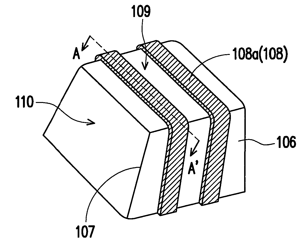
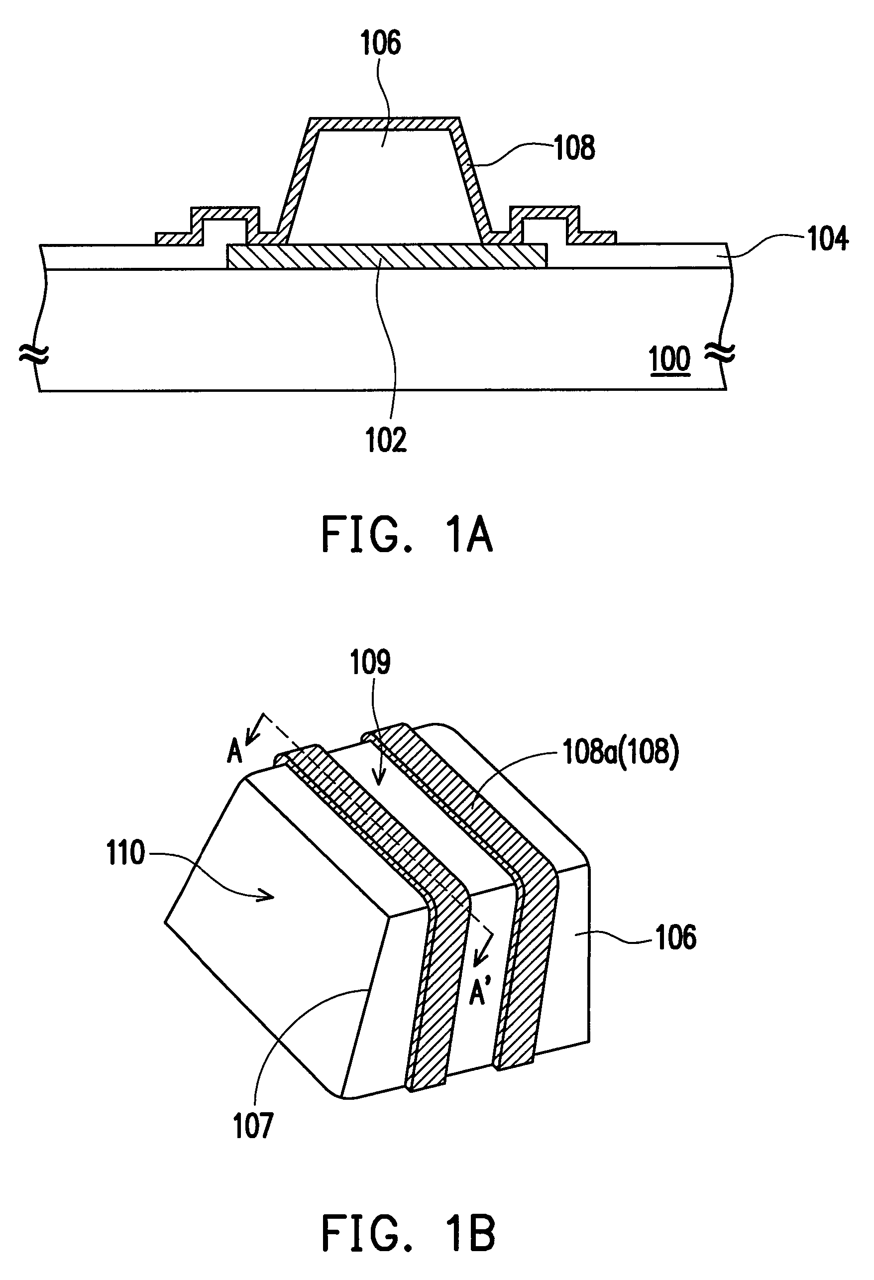
[0023]FIG. 1A is a lateral cross-sectional view showing an electrical connecting structure according to an embodiment of the present invention, and FIG. 1B is a solid schematic diagram illustrating a polymer bump and a patterned conductive layer of the electrical connecting structure shown in FIG. 1A. The cross-sectional view of FIG. 1A corresponds to cross-sectional line A-A′ in FIG. 1B. Referring to FIG. 1A and FIG. 1B, the electrical connecting structure in this embodiment comprises a conductive pad 102, a polymer bump 106, and a patterned conductive layer 108.

[0024]The conductive pad 102 is disposed on a substrate 100. In a preferred embodiment, the substrate 100 further comprises a protective layer 104 covering thereon and exposing the conductive pad 102. The substrate 100 is, for example, a glass substrate, a silicon substrate, a plastic substrate, or a metal substrate. The conductive pad 102 is, for example, a metal conductive pad which is electrically connected with elements...


PUM


Abstract

An electrical connecting structure including a conductive pad, a polymer bump and a patterned conductive layer is provided. The conductive pad is on a substrate and the polymer bump is disposed over the substrate. The patterned conductive layer is disposed on the polymer bump and electrically connects to the conductive pad, wherein the patterned conductive layer covers a portion of the polymer bump and exposes another portion of the polymer bump.

Description

CROSS-REFERENCE TO RELATED APPLICATION[0001]This application claims the priority benefit of Taiwan application serial no. 97104832, filed on Feb. 12, 2008. The entirety of the above-mentioned patent application is hereby incorporated by reference herein and made a part of specification.BACKGROUND OF THE INVENTION[0002]1. Field of the Invention[0003]The present invention relates to an electrical connecting structure and a electronic device bonding structure, and particularly relates to a low stress connecting structure and a bonding structure which using this structure.[0004]2. Description of Related Art[0005]As technology advances, all kinds of electronic devices are developed to be miniaturized and multi-function. Hence, high density assemble methods were developed to increase electrical signal transition.[0006]By conventional technique, anisotropic conductive film (ACF) is a popular connecting method using for electronic components connection such as semiconductor with the pattern...

Claims


Application Information

Patent Timeline
Patent Type & Authority Patents(United States)
IPC IPC(8): H01L23/48
CPCH01L23/49811H01L23/49866H01L24/13H01L24/11H01L2224/0401H01L2924/01082H01L2924/01033H01L2224/13008H01L2224/13541H01L2224/13578H01L2224/0235H01L2224/05567H01L2224/13007H01L2224/13017H01L2224/13022H01L2224/1319H01L2224/13566H01L2224/1357H01L2224/136H01L2224/16H01L2924/0002H01L2924/00013H01L2924/07802H01L2924/00014H01L2224/13099H01L2224/13599H01L2224/05599H01L2224/05099H01L2224/29099H01L2224/29599H01L2924/00H01L2224/05552H01L2924/15788
Inventor TSANG, NGAIKAO, KUO-SHU
Owner TAIWAN TFT LCD ASSOC
Why Eureka
Try Eureka