Stress management for tensile films

a stress management and tensile film technology, applied in the direction of coatings, metallic material coating processes, chemical vapor deposition coatings, etc., can solve the problems of dielectric material, dielectric material, dielectric material, structural features of the device having decreased spatial dimensions, etc., to reduce the tendency for subsequently deposited film, reduce the tendency for cracking, and facilitate the filling of trenches

Active Publication Date: 2011-05-03
APPLIED MATERIALS INC
View PDF168 Cites 47 Cited by
  • Summary
  • Abstract
  • Description
  • Claims
  • Application Information

AI Technical Summary

Benefits of technology

[0006]The formation of a gap-filling silicon oxide layer with reduced tendency towards cracking is described. The deposition involves the formation of a flowable silicon-containing layer which facilitates the filling of trenches. Subsequent processing at high substrate temperature causes less cracking in the dielectric film than flowable films formed in accordance with methods in the prior art. A compressive liner layer deposited prior to the formation of the gap-filling silicon oxide layer is described and reduces the tendency for the subsequently deposited film to crack. A compressive capping layer deposited after a flowable silicon-containing layer has also been determined to reduce cracking. Compressive liner layers and compressive capping layers can be used alone or in combination to reduce and often eliminate cracking. Compressive capping layers in disclosed embodiments have additionally been determined to enable an underlying layer of silicon nitride to be transformed into a silicon oxide layer.

Problems solved by technology

The decreasing feature sizes result in structural features on the device having decreased spatial dimensions.
The widths or gaps and trenches on the device narrow to a point where the aspect ratio of gap depth to its width becomes high enough to make it challenging to fill the gap with dielectric material.
The depositing dielectric material is prone to clog at the top before the gap completely fills, producing a void or seam in the middle of the gap.
However, once these highly flowable materials are deposited, they have to be hardened into a solid dielectric material.
Unfortunately, the departing carbon and hydroxyl species often leave behind pores in the hardened dielectric that reduce the quality of the final material.
In addition, the hardening dielectric also tends to shrink in volume, which can leave cracks and spaces at the interface of the dielectric and the surrounding substrate.

Method used


Image

  • Stress management for tensile films
  • Stress management for tensile films
  • Stress management for tensile films

Examples


Embodiment Construction

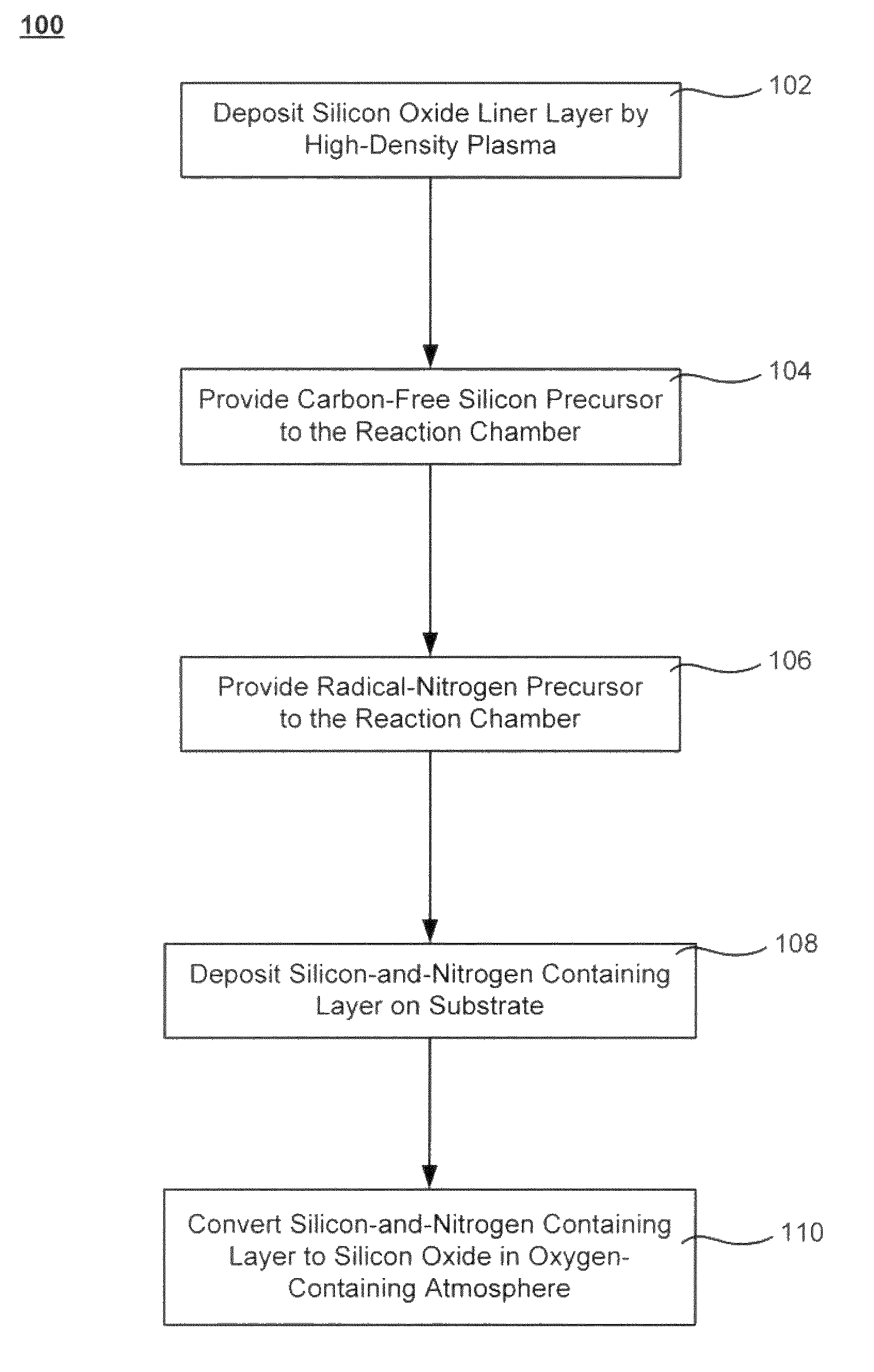
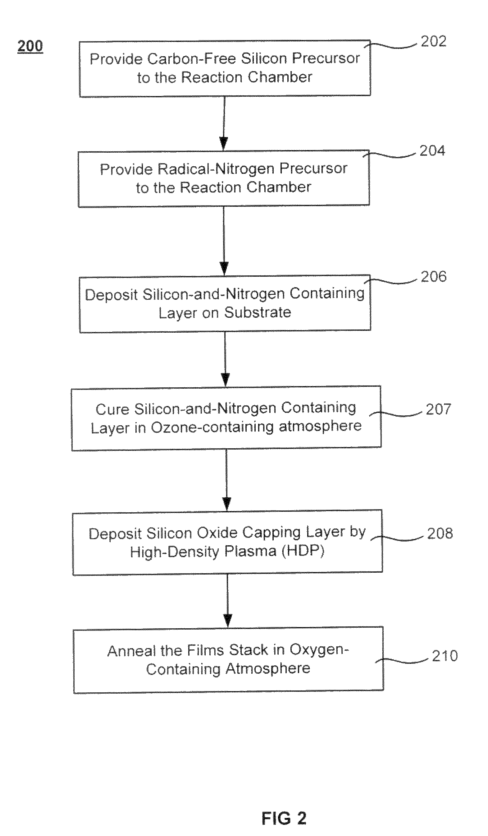
[0018]The formation of a gap-filling silicon oxide layer with reduced tendency towards cracking is described. The deposition involves the formation of a flowable silicon-containing layer which facilitates the filling of trenches. Subsequent processing at high substrate temperature causes less cracking in the dielectric film than flowable films formed in accordance with methods in the prior art. A compressive liner layer deposited prior to the formation of the gap-filling silicon oxide layer is described and reduces the tendency for the subsequently deposited film to crack. A compressive capping layer deposited after a flowable silicon-containing layer has also been determined to reduce cracking. Compressive liner layers and compressive capping layers can be used alone or in combination to reduce cracking. Compressive capping layers in disclosed embodiments have additionally been determined to enable an underlying layer of silicon nitride to be transformed into a silicon oxide layer....


PUM

PropertyMeasurementUnit
widthaaaaaaaaaa
feature sizesaaaaaaaaaa

Abstract

The formation of a gap-filling silicon oxide layer with reduced tendency towards cracking is described. The deposition involves the formation of a flowable silicon-containing layer which facilitates the filling of trenches. Subsequent processing at high substrate temperature causes less cracking in the dielectric film than flowable films formed in accordance with methods in the prior art. A compressive liner layer deposited prior to the formation of the gap-filling silicon oxide layer is described and reduces the tendency for the subsequently deposited film to crack. A compressive capping layer deposited after a flowable silicon-containing layer has also been determined to reduce cracking. Compressive liner layers and compressive capping layers can be used alone or in combination to reduce and often eliminate cracking. Compressive capping layers in disclosed embodiments have additionally been determined to enable an underlying layer of silicon nitride to be transformed into a silicon oxide layer.

Description

CROSS-REFERENCES TO RELATED APPLICATIONS[0001]This application is related to U.S. Prov. Pat. App. Ser. No. 61 / 231,729, filed Aug. 6, 2009, and titled “FORMATION OF SILICON OXIDE USING NON-CARBON FLOWABLE CVD PROCESSES,” the entire contents of which is herein incorporated by reference for all purposes.BACKGROUND OF THE INVENTION[0002]Semiconductor device geometries have dramatically decreased in size since their introduction several decades ago. Modern semiconductor fabrication equipment routinely produces devices with 250 nm, 180 nm, and 65 nm feature sizes, and new equipment is being developed and implemented to make devices with even smaller geometries. The decreasing feature sizes result in structural features on the device having decreased spatial dimensions. The widths or gaps and trenches on the device narrow to a point where the aspect ratio of gap depth to its width becomes high enough to make it challenging to fill the gap with dielectric material. The depositing dielectric...

Claims


Application Information

Patent Timeline
Patent Type & Authority Patents(United States)
IPC IPC(8): H01L21/31H01L21/469
CPCC23C16/401C23C16/452C23C16/56H01L21/02164H01L21/0217H01L21/02274H01L21/76837H01L21/02326H01L21/02362H01L21/31608H01L21/3185H01L21/76829H01L21/76834H01L21/02304
Inventor LIANG, JINGMEIPATEL, ANJANA M.INGLE, NITIN K.VENKATARAMAN, SHANKAR
Owner APPLIED MATERIALS INC
Why Eureka
Try Eureka