System and method for integrated circuit planar netlist interpretation

a technology of integrated circuits and netlists, applied in the field of electronic devices and methods, can solve the problems of large cost, large time consumption, and complex tasks, and achieve the effects of reducing the cost of implementation, and increasing the complexity of the task

Inactive Publication Date: 2011-05-03
INFINEON TECH AG
View PDF21 Cites 43 Cited by
  • Summary
  • Abstract
  • Description
  • Claims
  • Application Information

AI Technical Summary

Problems solved by technology

Reverse engineering and patent infringement analysis, however, generally are very complex tasks that can take significant time and incur large costs.
One factor that increases the complexity of the reverse engineering task is that detailed information about the integrated circuit is determined primarily from the physical chip, without access to the information generated by the design process.

Method used


Image

  • System and method for integrated circuit planar netlist interpretation
  • System and method for integrated circuit planar netlist interpretation
  • System and method for integrated circuit planar netlist interpretation

Examples


Embodiment Construction

[0050]The making and using of the presently preferred embodiments are discussed in detail below. It should be appreciated, however, that the present invention provides many applicable inventive concepts that can be embodied in a wide variety of specific contexts. The specific embodiments discussed are merely illustrative of specific ways to make and use the invention, and do not limit the scope of the invention.

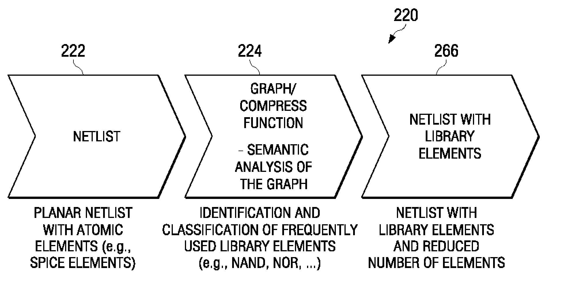
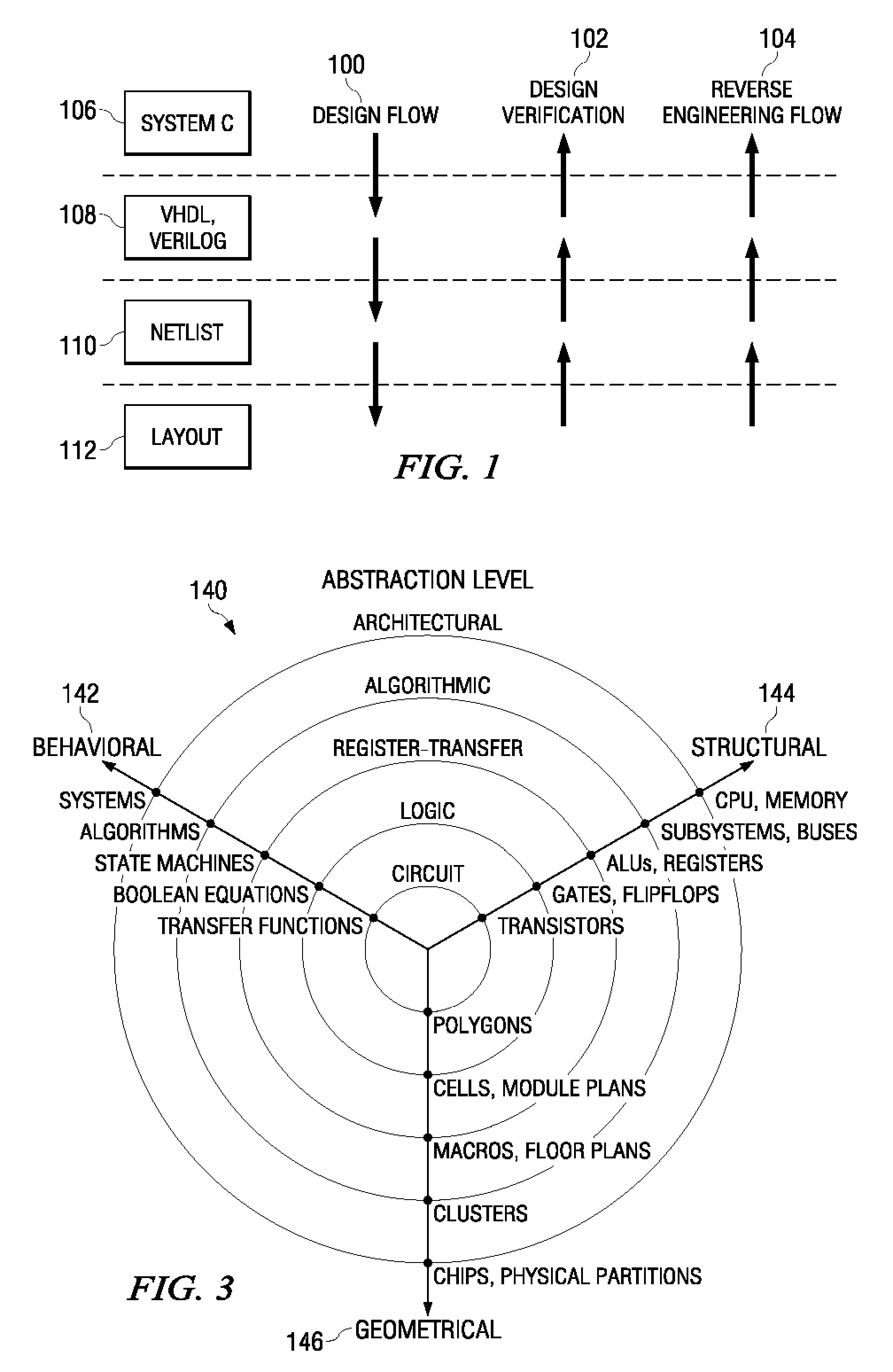
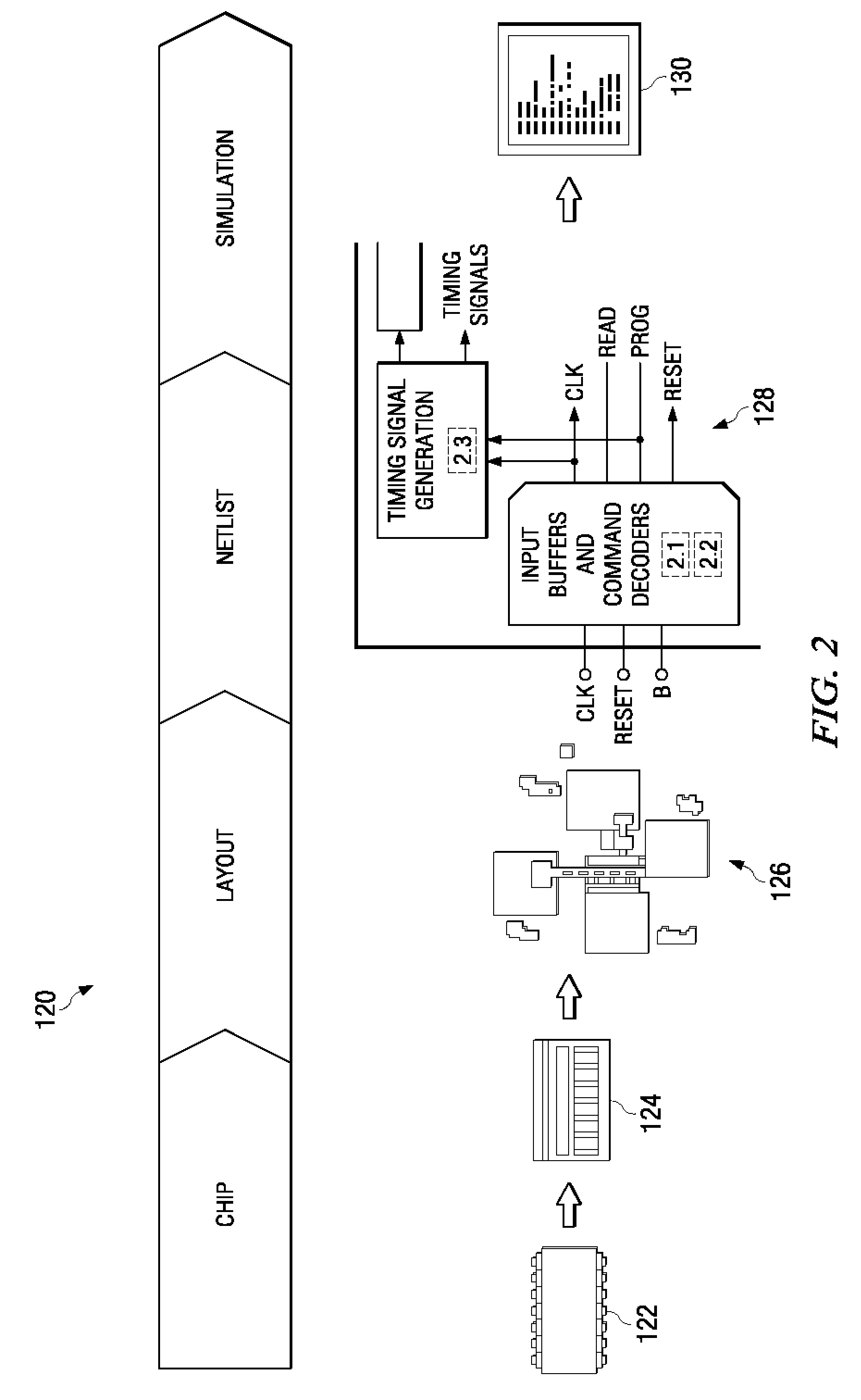
[0051]The present invention will be described with respect to preferred embodiments in a specific context, namely systems and methods for planar netlist interpretation in the reverse engineering of semiconductor-based integrated circuits (ICs). The invention also may be applied, however, to other types of integrated circuits and electronics, such as printed circuit boards, organic electronics, nanotechnology devices, microelectromechanical devices, and so forth. Furthermore, the invention also may be applied to other applications that may benefit from planar netlist interpret...


PUM


Abstract

Systems and methods for integrated circuit planar netlist interpretation are disclosed. In one embodiment, higher abstraction level descriptions of an integrated circuit are generated from a planar netlist and layout data of the integrated circuit. Various embodiments may derive the higher abstraction levels through, for example, netlist compression and netlist partitioning. Other embodiments may derive the higher abstraction levels using, for example, device and module hypothesis search functions based on device properties and design constraints derived from netlist and layout data.

Description

TECHNICAL FIELD[0001]This invention relates generally to electronic devices and methods, and more particularly to systems and methods for planar netlist interpretation, as used in, for example, reverse engineering or design verification of integrated circuits.BACKGROUND[0002]Integrated circuits are widely used in many electronic and other applications. An integrated circuit typically comprises many interconnected semiconductor devices, such as transistors, that are formed on a semiconductor wafer by depositing various types of materials on the semiconductor wafer, and patterning the thin films of material to form the devices and their connections. The design of an integrated circuit may include determining its functionality, schematics, modeling, material selection, and layout.[0003]After an integrated circuit has been designed, design verification may be performed to determine whether the circuit design meets its specifications and performs as intended. The design verification phas...

Claims


Application Information

Patent Timeline
Patent Type & Authority Patents(United States)
IPC IPC(8): G06F9/45
CPCG06F17/505G06F30/327
Inventor LIPPMANN, BERNHARDJUNGHANNS, ANDREAS
Owner INFINEON TECH AG
Why Eureka
Try Eureka