2,7-Carbazolenevinylene derivatives as novel materials in producing organic based electronic devices

a technology of carbazolene and derivatives, applied in thermoelectric devices, natural mineral layered products, nanoinformatics, etc., can solve the problems of preventing their utilization with plastic substrates, difficult processing, and easy oxidation in air

Inactive Publication Date: 2007-08-02
NAT RES COUNCIL OF CANADA
View PDF7 Cites 33 Cited by
  • Summary
  • Abstract
  • Description
  • Claims
  • Application Information

AI Technical Summary

Benefits of technology

[0013] Examples of mononuclear / polynuclear aromatic group are: phenylene, fluorene, naphthalene, anthracene, tetracene, pyrene, perylene, rubrene, phenanthrene, naphthylene, acenaphthene, fluoranthene and chrysene. Examples of mononuclear / polynuclear heterocyclic internal groups include 5-member heterocyclic groups such as furan, thiophene, pyrrole, oxazole, isooxazole, oxadiazoles, thiazole, isothiazole, imidazole, thiadiazole and pyrazole; 6-member heterocyclic groups such as pyridine, pyridazine, pyrimidine, pyrazine, triazine and tetrazine; benzo-fused ring systems such as benzooxazole, benzothiazole, benzimidazole, quinoline, isoquinoline, cinnoline, quinazoline, quinoxaline, phthalazine, benzothiadiazole and benzotriazine; polynuclear fused condensed ring systems such as phenazine, phenanthridine, acridine and diphenylene oxide. Examples of tertiary arylamine groups include triphenylamine, N,N′-diphenylbenzidine, N,N′-diphenyl-1,4-phenylenediamine and diphenylnaphthylamine. Olefinic, aromatic, heterocycle and tertiary arylamines groups may be substituted optionally with one or more substituants. Examples of substituants include C1-C20 linear or branched alkyl group, C1-C20 linear or branched alkoxy group, cyano, fluoro, chloro, bromo, iodo, C1-C20 linear or branched alkyloxycarbonyl, C1-C20 linear or branched aryloxycarbonyland poly (alkyleneoxy). Such substituants may be selected to improve the solubility or processing characteristics of the materials.

Problems solved by technology

However, the relatively high temperatures needed in their fabrication process prevent their utilization with plastic substrates.
Up to now, only pentacene and regioregular polythiophenes have demonstrated the required performances, but the former is difficult to process and the later is easily oxidized in air.
Current LCDs present limitations such as low efficiency, poor vision angle, and speed and temperature range limitations.
While some materials meet or exceed some of the requirements for commercial displays, to date none meets them all.

Method used


Image

  • 2,7-Carbazolenevinylene derivatives as novel materials in producing organic based electronic devices
  • 2,7-Carbazolenevinylene derivatives as novel materials in producing organic based electronic devices
  • 2,7-Carbazolenevinylene derivatives as novel materials in producing organic based electronic devices

Examples


first example

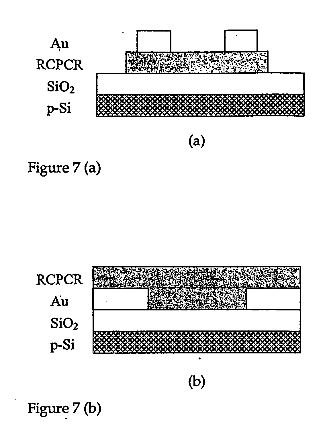
[0050] In a first embodiment of the present invention as shown in FIG. 7, an OFET was fabricated in the top contact geometry consisting of; a p-type silicon wafer covered with a thermally grown SiO2 film used as a substrate, a thin RCPCR semi-conductor layer, a source and drain gold electrode on top of the organic semi-conductor layer, and a gate electrode on the back side of the substrate. Prior to use, each substrate (15×15 mm2) is cleaned sequentially with acetone, ultrasonicated isopropanol at 80° C., and UV / ozone cleaner for 10 min. In order, the organic semi-conductor RCPCR and gold are deposited by thermal evaporation at a pressure of 1×10⁻⁷ torr at a substrate temperature of 25° C. for RCPCR and 25° C. for gold. The gold source and drain electrodes are deposited on top of the organic semi-conductor through a shadow mask forming a top contact geometry with a channel length of 40 μm and a channel width of 1 μm. An electrical wired bonded on the backside of the p-doped silicon ...

second example

[0052] In a second embodiment of the present invention as shown in FIG. 9, an OFET was fabricated in the top contact geometry consisting of; a p-type silicon wafer covered with a thermally grown SiO2 film used as a substrate, a thin CPC semi-conductor layer, a source and drain gold electrode on top of the organic semi-conductor layer, and a gate electrode on the back side of the substrate. Prior to use, each substrate (15×15 mm2) is cleaned sequentially with acetone, ultrasonicated isopropanol at 80° C., and UV / ozone cleaner for 10 min. Then, the substrate was treated suquentially in a NH4OH / H2O2 / H2O (2:2:100) solution for 15 min. H2O for 1 min, HCl / H2O2 / H2O (2:2:100) solution for 15 min, H2O for 1 min, dried with N2 and put in the UV / ozone cleaner for 1 h. Then, the surface of the substrate was treated with hexamethyldisilazane (HMDS) on a vapor prime system at 150° C. and 30 mmHg for 2 h prior to evaporation. In order, the organic semi-conductor CPC and gold are deposited by therm...

third example

[0054] In a third embodiment of the invention as shown in FIG. 12, an OLED was fabricated consisting of; an Indium Tin Oxide transparent conductive anode on a glass substrate, a thin PCVDPAP layer as emitter, and a Ca cathode. The Indium Tin Oxide coated glass (5×5 cm2) with a sheet resistance of 15 ohm / sq is patterned using photolithography techniques to produce ten segments each with an active area of 5×6 mm2. Prior to use, the substrates are cleaned sequentially with detergent, deionized water, acetone, ultrasonicated isopropanol at 60° C., and UV / ozone cleaner for 10 min. The polymeric PCVDPAP material is solubilized in chloroform, filtered through a 0.2 μm PTFE filter, spin-coated at 2000 rpm for 60 s onto the Indium Tin Oxide substrate, and dried at 40° C. for 10 min. The Ca layer is thermally evaporated at a pressure of 1×10⁻⁷ torr and at room temperature.

[0055] The OLED produced the electroluminescence spectrum shown in FIG. 13. The resulting diode emitted orange-red light ...


PUM

PropertyMeasurementUnit
temperatureaaaaaaaaaa
pressureaaaaaaaaaa
temperatureaaaaaaaaaa

Abstract

Organic Field Effect Transistor (OFET), an Organic Light Emitting Diode (OLED), an and an Organic Photovoltaic Cell (OPC) including as active material a congugated oligomeric or polymeric 2,7-carbazolenevinylene derivative described by the formula (I) or (II): Such OFETs, OLEDs and OPCs have improved devices properties and efficiencies.

Description

[0001] This application claims the benefit of U.S. Provisional Application 60 / 507,506 filed Oct. 1, 2003.FIELD OF THE INVENTION [0002] The present invention relates to the field of electronic and optoelectronic devices, and more particularly to organic based semi-conductor devices such as Organic Field Effect Transistors (OFETs), Organic Light Emitting Diodes (OLEDs) and Organic Photovoltaic Cells (OPCs). BACKGROUND [0003] Organic conjugated oligomers and polymers are materials that possess a delocalized pi-electron system along their backbone. These organic materials are subject to important investigations from both academic and industrial laboratories due to their great potential for applications in electronic and opto-electronic devices, such as field effect transistors (OFETs), light emitting diodes (OLEDs) and photovoltaic cells (OPCs). The economical advantages of using organic over inorganic semi-conducting materials in devices include, low cost of synthesis, ease of processi...

Claims


Application Information

Patent Timeline
Patent Type & Authority Applications(United States)
IPC IPC(8): H01L51/00C08G61/12H01L51/30H01L51/40H01L51/50
CPCB82Y10/00Y02E10/549C08G73/0672H01L51/0012H01L51/0035H01L51/0037H01L51/0038H01L51/0043H01L51/0059H01L51/0072H01L51/0525H01L51/0545H01L51/0558H01L51/42H01L51/4253H01L51/5012H01L51/5048C08G61/124
Inventor DROLET, NICOLASMORIN, JEAN-FRANCOISTAO, YELECLERC, MARIOSIROIS, KATHLEEN
Owner NAT RES COUNCIL OF CANADA
Why Eureka
Try Eureka