Semiconductor device including mounting board with stitches and first and second semiconductor chips

a technology of semiconductor chips and mounting boards, applied in semiconductor devices, semiconductor/solid-state device details, electrical apparatus, etc., can solve the problems of complicated arrangement of bonding wires, increased package size, and increased package area, so as to suppress the increase in package size, reduce the connection distance between each chip select pad and each second stitch, and increase the package area

Active Publication Date: 2011-05-17
RENESAS ELECTRONICS CORP
View PDF11 Cites 11 Cited by
  • Summary
  • Abstract
  • Description
  • Claims
  • Application Information

AI Technical Summary

Benefits of technology

[0032]Thus, in one embodiment, the chip select pads are arranged on the end of each line of the electrode pads, and the chip select pads are wired to the stitches that are arranged along a direction different from that in which the electrode pads are arranged. As a result, in each chip, a connection distance between each chip select pad and each second stitch can be reduced. Further, the second stitches are arranged in a direction different from that in which the first stitches are arranged. Accordingly, even when a plurality of semiconductor chips are stacked on top of each other, the wire connecting each chip select pad and each second stitch to each other can be prevented from striding over or intersecting another wire connected to the electrode pad of the chip select pad, for example. As a result, the necessary space to be secured so as to prevent the wires from being brought into contact with each other can be reduced in size. Therefore, also in the case of stacking a plurality of memory chips on top of each other, it is possible to suppress the increase in package size which is determined depending on a balance among an area of a chip mounting region on one surface of the mounting board, an area of a stitch forming region, an area and a thickness of a region necessary for preventing the wires from being brought into contact with each other, and the like.

Problems solved by technology

Further, in the structure disclosed in 2005-302871 A, when the number of pad lines on the substrate is to be simply reduced, there is a fear that the arrangement of bonding wires are complicated and the wires are brought into contact with each other.
Further, there is another fear that, in order to prevent the wires from being brought into contact with each other, the package is increased in size.
As a result, as shown in FIG. 13, the wire connecting the chip select pad and the stitch on the board to each other strides over or intersects another wire in some areas, which complicates the wiring.
Accordingly, it is necessary to sufficiently secure a space for preventing the wires from being brought into contact with each other, which becomes a cause of the increase in size of the package.
Further, in order to prevent the wires from intersecting each other, when a line of stitches is formed for each chip as disclosed in 2005-302871 A, it is necessary to provide a large space for forming the lines of the stitches on the mounting board, which results in the increase in size of the package.

Method used


Image

  • Semiconductor device including mounting board with stitches and first and second semiconductor chips
  • Semiconductor device including mounting board with stitches and first and second semiconductor chips
  • Semiconductor device including mounting board with stitches and first and second semiconductor chips

Examples


first embodiment

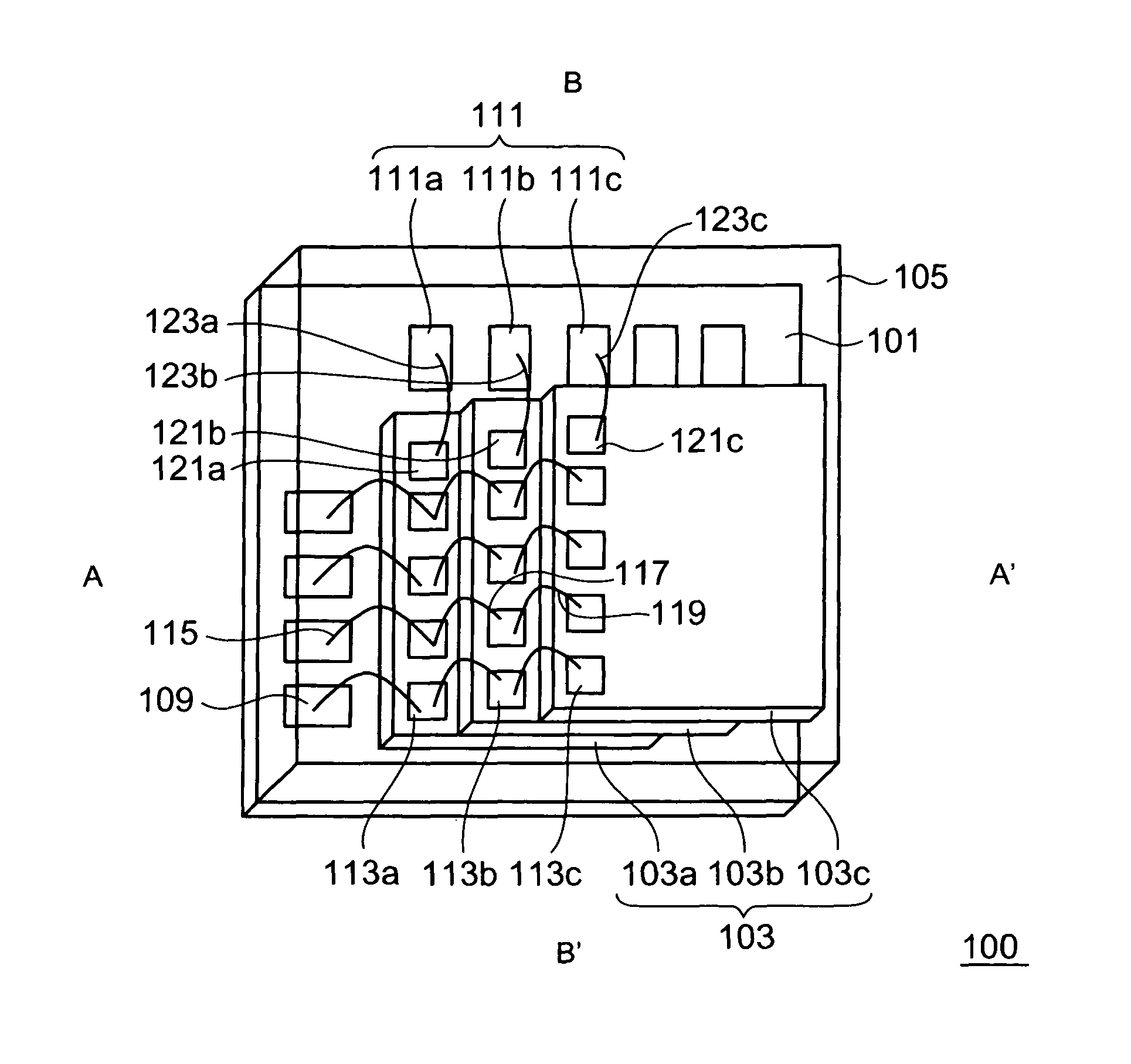
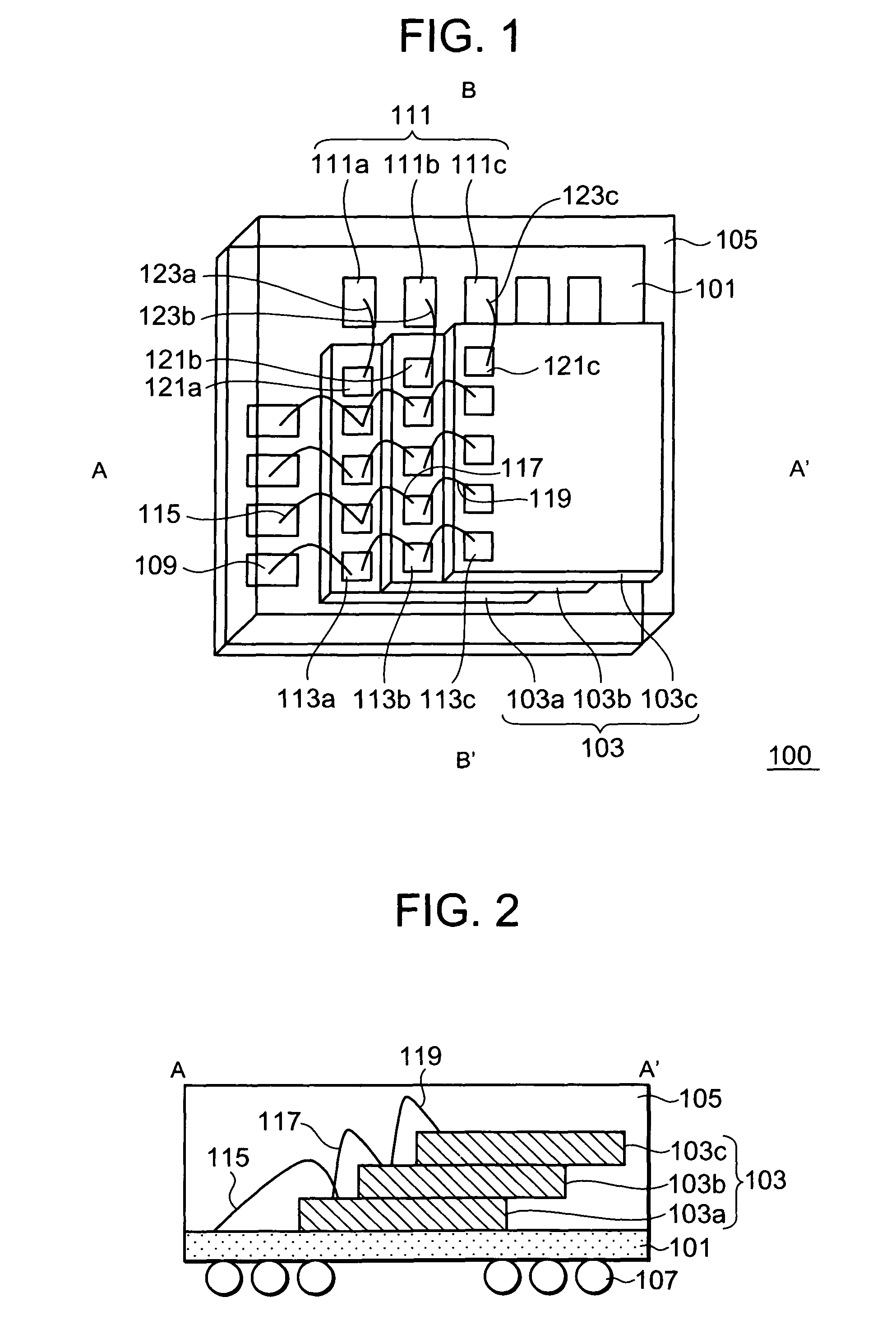
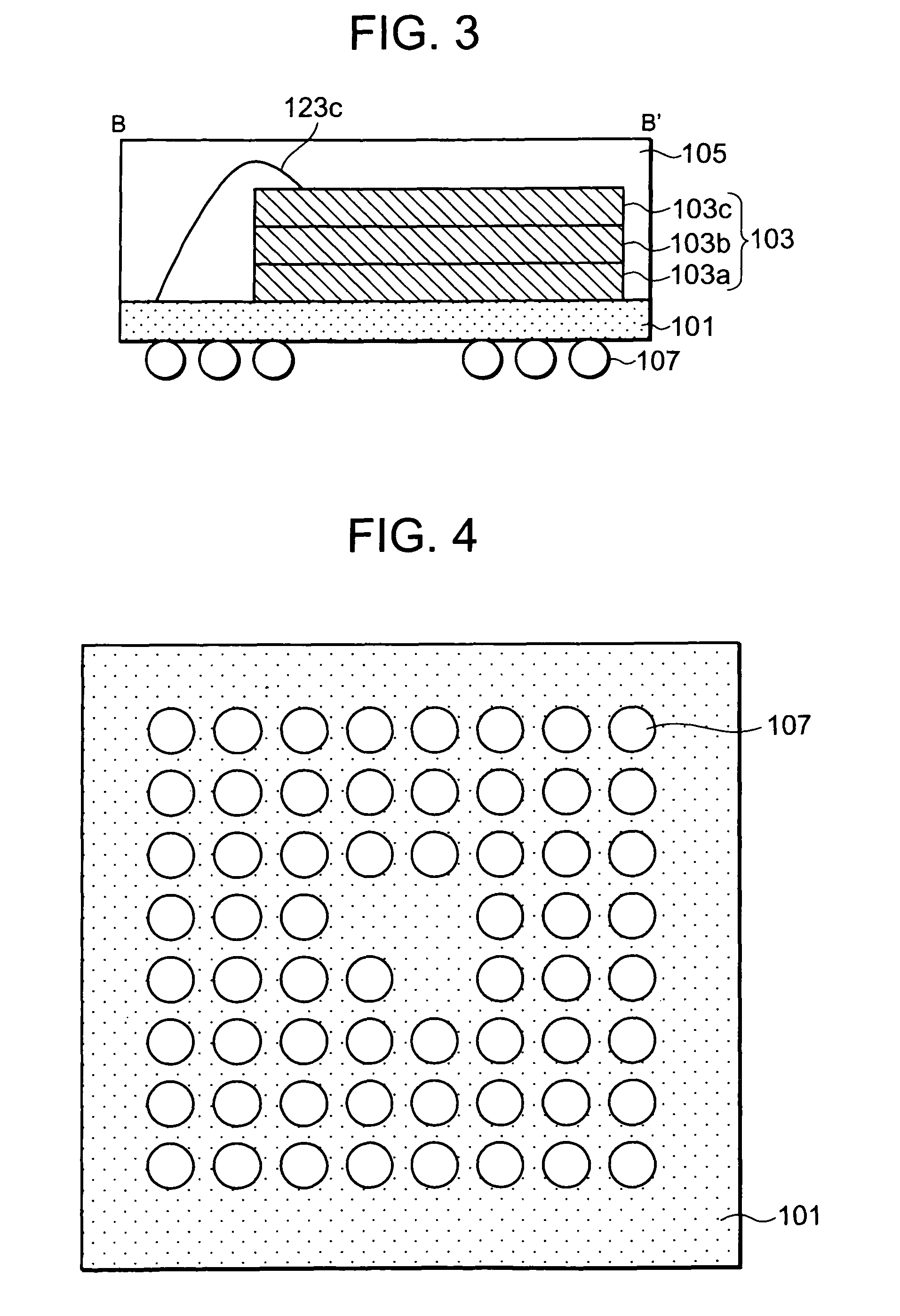
[0051]FIG. 1 is a perspective view showing a structure of a semiconductor package according to a first embodiment of the present invention. FIG. 2 is a cross-sectional diagram of the semiconductor package taken along the line A-A′ of FIG. 1. FIG. 3 is a cross-sectional diagram of the semiconductor package taken along the line B-B′ of FIG. 1. FIG. 4 is a plan view showing a back surface of a semiconductor package 100 shown in FIG. 1.

[0052]As shown in FIGS. 1 to 4, a semiconductor device (semiconductor package 100) according to the first embodiment of the present invention includes a first memory chip and a second memory chip (first memory chip 103a and second memory chip 103b) mounted in the stated order from below on one surface (chip mounting surface) of a mounting board 101. The semiconductor package 100 further includes a third memory chip 103c mounted on the second memory chip 103b. Hereinafter, the first memory chip 103a, the second memory chip 103b, and the third memory chip 1...

second embodiment

[0084]FIG. 8 is a cross-sectional diagram showing a structure of a semiconductor package according to a second embodiment of the present invention. A basic structure of a semiconductor package 110 shown in FIG. 8 is similar to that of the semiconductor package 100 (see FIG. 2) according to the first embodiment of the present invention. However, the semiconductor package 110 is different from the semiconductor package 100 in that the side adjacent to the second stitches 111, that is, the side adjacent to the side on which the electrode pads are formed, of the chip positioned in the upper layer is shorter than that of the chip positioned in the lower layer.

[0085]Also in the semiconductor package 110, as in the case of the semiconductor package 100, the length of the side of each of the first memory chip 103a, the second memory chip 103b, and the third memory chip 103c, on which the electrode pads are arranged, is the same. Also in the semiconductor package 110, when viewed from above ...

third embodiment

[0090]FIG. 10 is a plan view showing a structure of a semiconductor package according to a third embodiment of the present invention. FIG. 11 is a cross-sectional diagram of the semiconductor package taken along the line A-A′ of FIG. 10.

[0091]A basic structure of a semiconductor package 120 shown in FIGS. 10 and 11 is similar to that of the semiconductor package 100 shown in FIGS. 1 to 3. However, the semiconductor package 120 further includes a fourth memory chip 103d stacked on the third memory chip 103c. The first memory chip 103a, the second memory chip 103b, the third memory chip 103c, and the fourth memory chip 103d each have the same planar shape and each include the electrode pads arranged in the same manner. On each of the first memory chip 103a and the third memory chip 103c, the electrode pads are arranged in a single line along the same side. The line of the electrode pads of each of the second memory chip 103b and the fourth memory chip 103d is formed on a side opposite...


PUM


Abstract

A first memory chip (103a) and a second memory chip (103b) mounted in this order on one surface of a mounting board (101) each have a rectangular planar shape and include a plurality of electrode pads formed in a single line along one side of the rectangle. An electrode pad line of the second memory chip (103b) is formed in parallel with an electrode pad line of the first memory chip (103a). A chip select pad is disposed on an end of the electrode pad line. Control pads, address pads, or data pads (113a) of the first memory chip (103a) are wire bonded to first stitches (109) formed in a single line along one side of the rectangle. A chip select pad (121a) and a chip select pad (121b) are wire bonded to second stitches (111) formed in a line along a side adjacent to a side of the chip select pad (121a). Accordingly, an increase in package area is suppressed when a plurality of memory chips are stacked.

Description

BACKGROUND OF THE INVENTION[0001]1. Field of the Invention[0002]The present invention relates to a semiconductor device, and more particularly, to a system-in-package (SiP) technology.[0003]2. Description of the Related Art[0004]Various stack-type semiconductor devices and bonding methods therefor have been discussed.[0005]As an example thereof, a technology for connecting a memory chip to a lead terminal of a lead frame is disclosed in each of JP 11-054693 A, JP 11-074451 A, and JP 2000-332194 A.[0006]JP 11-054693 A and JP 11-074451 A each disclose a semiconductor device having a first semiconductor chip and a second semiconductor chip stacked in the stated order on an island. The first and second semiconductor chips are memory chips. The second semiconductor chip, which is slightly smaller than the first semiconductor chip, is mounted on a central portion of the first semiconductor chip, and two opposing sides of the first semiconductor chip are exposed from the second semiconduct...

Claims


Application Information

Patent Timeline
Patent Type & Authority Patents(United States)
IPC IPC(8): H01L23/48
CPCH01L24/49H01L25/0657H01L23/3128H01L2224/32145H01L2224/48091H01L2224/48145H01L2224/48227H01L2224/4903H01L2224/49051H01L2224/4911H01L2224/49111H01L2224/49113H01L2224/49175H01L2225/06506H01L2225/0651H01L2225/06562H01L2924/01004H01L2924/01005H01L2924/01015H01L2924/01058H01L2924/01082H01L2924/15311H01L2924/30105H01L24/48H01L2224/32225H01L2224/73265H01L2924/01006H01L2924/01024H01L2924/01033H01L2924/01055H01L2924/00014H01L2924/00H01L2924/00012H01L24/73H01L2924/181H01L2224/05554H01L2224/45099H01L2224/05599
Inventor SASAKI, KOU
Owner RENESAS ELECTRONICS CORP
Why Eureka
Try Eureka