Charged particle beam apparatus for forming a specimen image

a charge particle and specimen image technology, applied in the direction of material analysis, instruments, and wave/particle radiation, can solve the problems of difficult to prevent image errors at the edge of defect image search, difficult to improve the contrast of display image, and inability to reduce image errors. the effect of preventing image errors

Active Publication Date: 2011-06-07
HITACHI HIGH-TECH CORP
View PDF12 Cites 5 Cited by
  • Summary
  • Abstract
  • Description
  • Claims
  • Application Information

AI Technical Summary

Benefits of technology

[0007]In the technique disclosed in JP-A No. 2004-227886, a defect position is searched from an acquired defect image for search such that the scan area of an electron beam is matched with the display area of the acquired image, and then the acquired image is trimmed such that the scan area of the electron beam corresponds with the scan area when the defect image for search is captured, thereby acquiring the defect image for observation. FIG. 2 is a diagram illustrating the relationship between the display image and the acquired image when the defect image for observation is acquired. Scanning 104 with an electron beam is performed on a pattern 101 formed on a specimen in the direction of an arrow, thereby acquiring an acquired image 103, and a necessary area is trimmed out from the acquired image to obtain a display image 102. In this technique, the capture magnification of the acquired image 103 is the same as that of the defect image for search. In this technique, since the edge of the defect image for observation does not correspond to the boundary between the area in which the electron beam is radiated and the area in which no electron beam is radiated, it is possible to prevent image errors in the edge of the image, but it is difficult to prevent image errors at the edge of the defect image for search. In the technique disclosed in JP-A No. 11-120951, since the technique shown in FIG. 2 can be applied to all the display images, it is possible to prevent image errors at the edge of the display image of the defect image for search. However, these techniques cannot reduce image errors, such as brightness variation, caused from the relationship between the structure or the arrangement of a pattern and the scan direction of the charged particle beam.
[0010]An object of the invention is to provide a charged particle beam apparatus capable of preventing an image error in a display image, capturing a clear image without brightness variation, improving a defect recognition rate during auto review, and preventing erroneous recognition of display information.
[0013]According to the above-mentioned aspect of the invention, it is possible to provide a charged particle beam apparatus capable of preventing image errors occurring at, for example, the boundary between a charged-up area and a neutron area in a display image, and acquiring a clear image without brightness variation.

Problems solved by technology

In this technique, since the edge of the defect image for observation does not correspond to the boundary between the area in which the electron beam is radiated and the area in which no electron beam is radiated, it is possible to prevent image errors in the edge of the image, but it is difficult to prevent image errors at the edge of the defect image for search.
However, these techniques cannot reduce image errors, such as brightness variation, caused from the relationship between the structure or the arrangement of a pattern and the scan direction of the charged particle beam.
However, in the technique, since the electron beam radiated by the above-mentioned method is not used as a display image, it is difficult to improve the contrast of the display image.
When the display direction varies, erroneous recognition of display information is likely to occur in an image having directivity such as bump / bent information.

Method used


Image

  • Charged particle beam apparatus for forming a specimen image
  • Charged particle beam apparatus for forming a specimen image
  • Charged particle beam apparatus for forming a specimen image

Examples


first embodiment

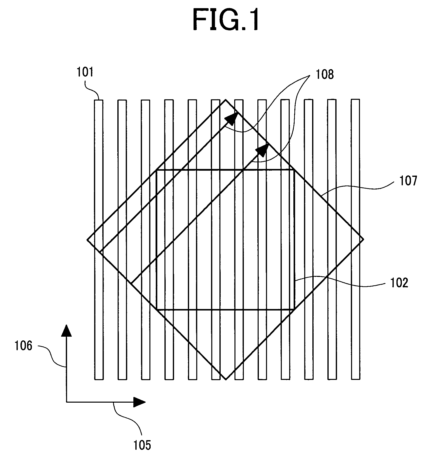
[0027]As a first embodiment, a defect review system in which the inclination angle of the scan direction of charged particle beams is fixed will be described. The defect review system means a charged particle beam apparatus that acquires (reviews) high-resolution image information of defects of interest on a specimen to be reviewed. In many cases, an inspection apparatus other than an appearance inspection apparatus is generally used to detect positional information of an important position to be inspected, and a review operation is performed on the basis of the positional information. As the specimen to be reviewed, semiconductor wafers having a circuit pattern formed thereon are generally used, but bare wafers without patterns, chips or pieces divided from wafers, or liquid crystal panels or magnetic disk media may be used as the specimen. Examples of the important position to be reviewed include positions where electric defects, such as the breaking of lines or defects in contact...

second embodiment

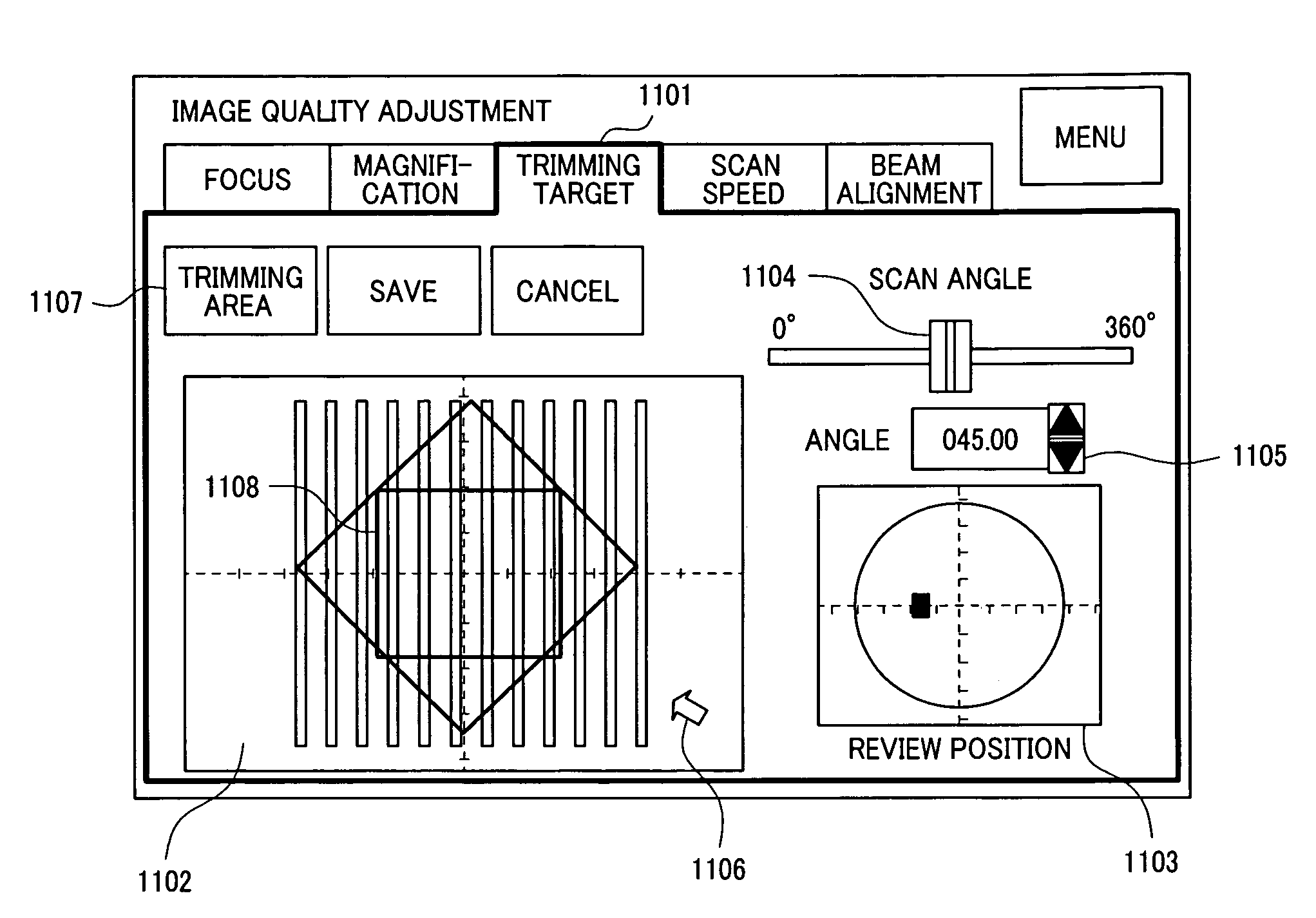
[0050]Next, as a second embodiment, a process of complementing pixels when a defect review system displays an image will be described. In the second embodiment, the configuration of an apparatus, the overall process flow of a defect review system, and a method of scanning a specimen with an electron beam are the same as those in the first embodiment, and thus a description thereof will be omitted. In addition, in this embodiment, the scan angle θ may be an arbitrary value, and a process of complementing pixels of a display image is performed according to the scan angle θ, if necessary.

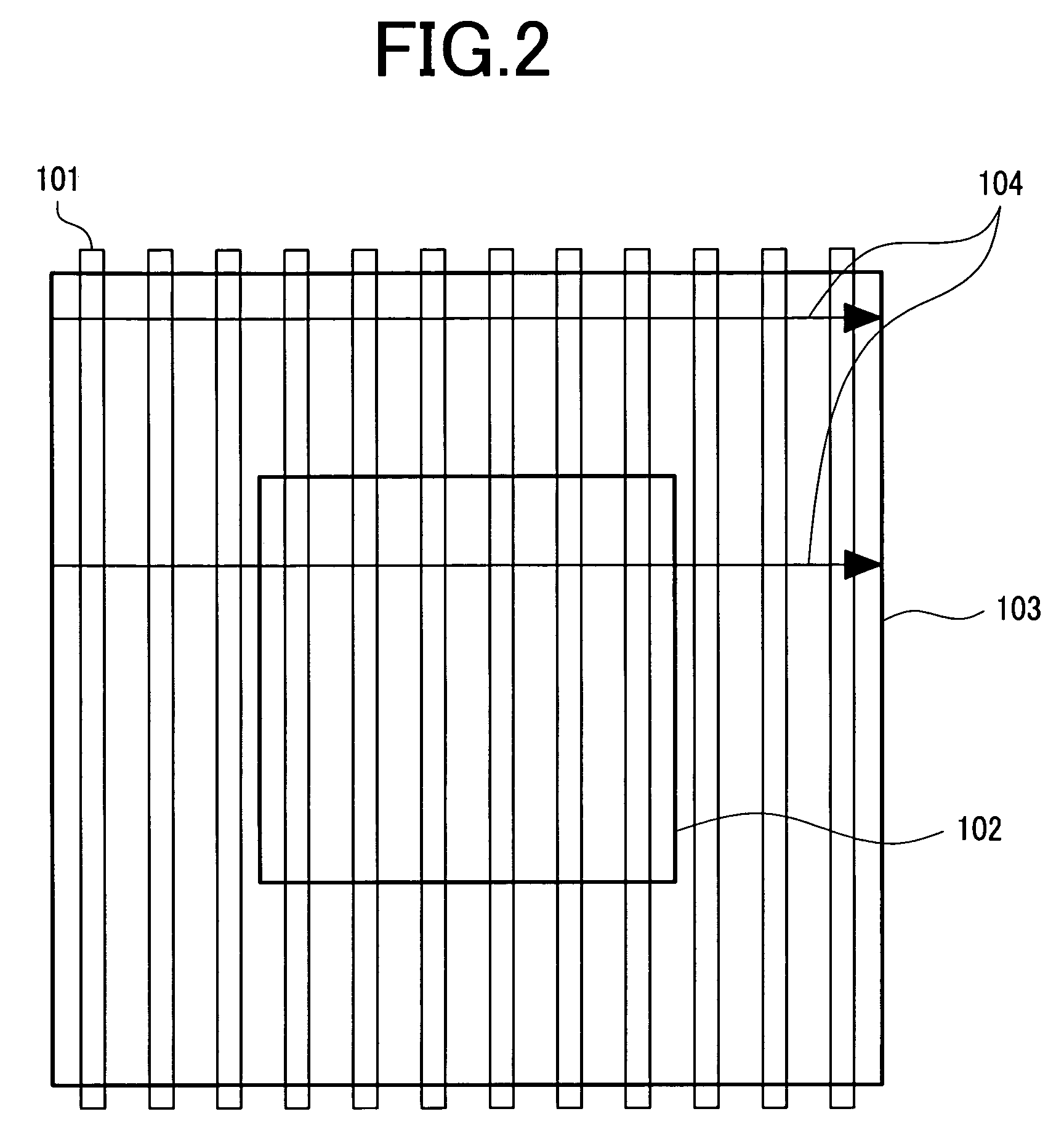
[0051]FIG. 9 shows acquired pixel information addresses and acquired image information addresses. In this embodiment, a rectangular coordinate is used, which is determined by wafer alignment and includes a first coordinate axis 136 (which corresponds to reference numeral 105 of FIG. 1) and a second coordinate axis 137 (which corresponds to reference numeral 106 of FIG. 1) orthogonal to the first coordi...


PUM


Abstract

The invention provides a charged particle beam apparatus capable of preventing image errors in a display image and capturing a clear display image. A display image displayed on a display unit has a rectangular shape having sides that are substantially parallel to coordinate axes of a rectangular coordinate system determined by wafer alignment. A charged particle beam is radiated onto an area including a display image in a direction that is not parallel to the coordinate axes of the reference rectangular coordinate system to scan the area. Then, among image information obtained by scanning, only information of a position within the display image is displayed on the image display unit. In this way, a clear display image without brightness variation is obtained.

Description

CLAIM OF PRIORITY[0001]The present application claims priority from Japanese patent application JP 2007-151752 filed on Jun. 7, 2007, the content of which is hereby incorporated by reference into this application.BACKGROUND OF THE INVENTION[0002]1. Field of the Invention[0003]The present invention relates to a charged particle beam apparatus, and more particularly, to a technique for measuring the shape and dimensions of a circuit pattern formed on a specimen or inspecting the circuit pattern.[0004]2. Description of the Related Art[0005]A technique for inspecting or reviewing the state of a circuit pattern formed on a semiconductor wafer is important to improve the yield and reliability of the products. The inspection or review is performed by an apparatus using light or an apparatus using charged particle beams, such as electron beams. In particular, in recent years, with the size reduction of semiconductor devices, the inspection and review processes using charged particle beams h...

Claims


Application Information

Patent Timeline
Patent Type & Authority Patents(United States)
IPC IPC(8): H01J37/26
CPCG01N23/225H01J37/28H01J37/265H01J2237/221
Inventor TAKAHASHI, NORITSUGUFUKUDA, MUNEYUKITODOKORO, HIDEOSATO, MITSUGU
Owner HITACHI HIGH-TECH CORP
Why Eureka
Try Eureka