Thermal interface material design for enhanced thermal performance and improved package structural integrity

a technology of thermal interface material and thermal insulation, applied in the field of electronic packaging, can solve the problems of poor heat transfer and inability to tolerate mechanical or thermal stresses

Active Publication Date: 2011-06-07
TEXAS INSTR INC
View PDF8 Cites 34 Cited by
  • Summary
  • Abstract
  • Description
  • Claims
  • Application Information

AI Technical Summary

Problems solved by technology

Such uncoupling can be caused by, e.g., mechanical or thermal stresses imposed on the device package.
Existing methods of coupling devices to a package involve the use of flexible materials, which can tolerate mechanical or thermal stresses, but which have poor heat transfer, or, the use of brittle materials, which have good heat transfer, but cannot tolerate mechanical or thermal stresses.

Method used


Image

  • Thermal interface material design for enhanced thermal performance and improved package structural integrity
  • Thermal interface material design for enhanced thermal performance and improved package structural integrity
  • Thermal interface material design for enhanced thermal performance and improved package structural integrity

Examples


Embodiment Construction

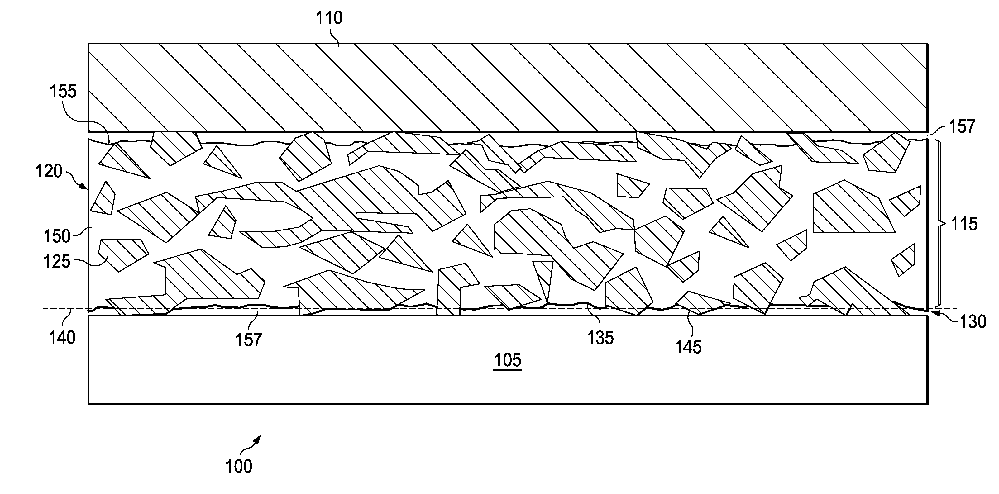
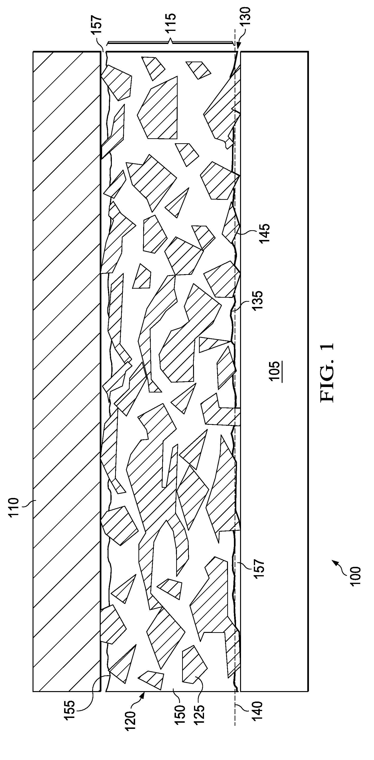
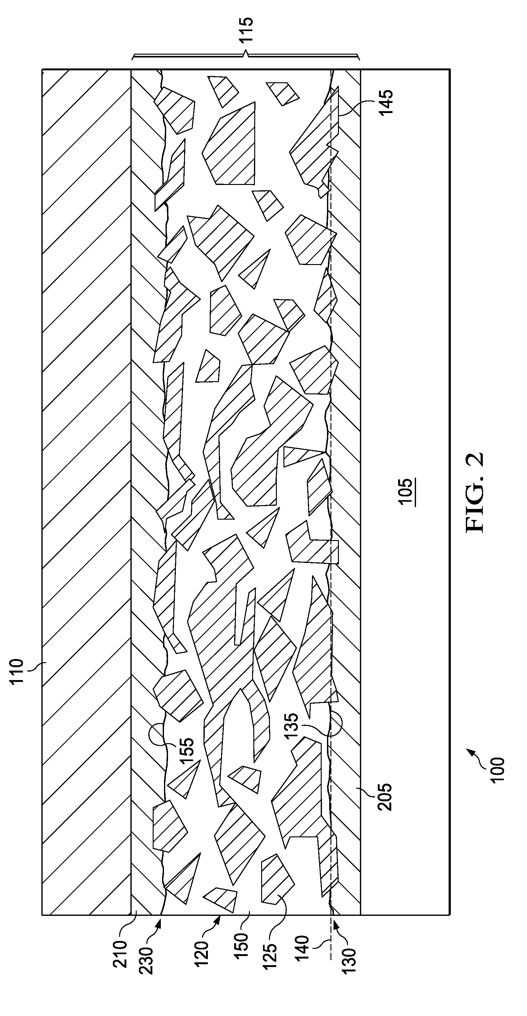
The disclosure is based at least in part on the recognition that a composition of highly conductive particles suspended in a resin can provide a desirable combination of high thermal conductivity and flexible coupling of a semiconductor device to a packaging component. Unfortunately, merely forming a resin layer with such particles suspended therein may not provide the desired amount heat transfer. It was found, as part of this disclosure, that poor heat transfer to and from the particle-containing resin layer can be due to the surface of the layer being rich in resin. That is, the resin-rich surface can deter the efficient transfer of heat into or out of the layer. It was further discovered, as part of this disclosure, that removing portions of the resin at the surface, such that a portion of the particles are exposed at the surface, improves heat transfer.

FIG. 1 presents a cross-sectional view of an example electronic package 100 of the disclosure. The package 100 comprises a semi...


PUM

PropertyMeasurementUnit
volume percentaaaaaaaaaa
diameteraaaaaaaaaa
diametersaaaaaaaaaa

Abstract

An electronic package comprising a semiconductor device, a heat spreader layer, and a thermal interface material layer located between the semiconductor device and the heat spreader layer. The thermal interface material layer includes a resin layer having heat conductive particles suspended therein. A portion of the particles are exposed on at least one non-planar surface of the resin layer such that the portion of exposed particles occupies a majority of a total area of a horizontal plane of the non-planar surface.

Description

TECHNICAL FIELDThe disclosure is directed, in general, to electronic packages such as used in electrical devices, and their method of manufacture.BACKGROUNDAfter the manufacture of a semiconductor device, there remains the need to package and mount the device to a surface to provide connections to other devices, and to protect the device from damage. Additionally, the mounting surface and protective covering can provide a means to dissipate heat from the device.It is increasingly important to have efficient heat transfer from semiconductor devices, as device power densities increase and device package form-factors decrease. It is also important to avoid damaging, and to prevent uncoupling of, the semiconductor devices from other components of the package. Such uncoupling can be caused by, e.g., mechanical or thermal stresses imposed on the device package. Existing methods of coupling devices to a package involve the use of flexible materials, which can tolerate mechanical or thermal...

Claims


Application Information

Patent Timeline
Patent Type & Authority Patents(United States)
IPC IPC(8): H01L23/34
CPCH01L23/293H01L23/373H01L23/3737H01L23/433H01L23/49513H01L24/29H01L24/32H05K3/305H01L2224/16225H01L2224/32245H01L2224/48247H01L2224/4826H01L2224/48472H01L2224/73253H01L2224/73265H01L2924/01005H01L2924/01027H01L2924/01029H01L2924/01047H01L2924/0105H01L2924/01078H01L2924/01079H01L2924/01082H01L2924/01327H01L2924/14H01L2924/15311H01L2924/16152H01L2924/19041H01L2924/19042H01L2924/19043H05K1/0203H05K2201/0209H01L24/48H01L2224/29H01L2224/2919H01L2924/01006H01L2924/01033H01L2924/014H01L2924/0665H01L2224/29101H01L2924/00013H01L2224/32225H01L2224/2929H01L2224/29311H01L2224/29339H01L2224/29344H01L2224/29347H01L2224/29393H01L2224/16227H01L2224/29499H01L2924/00H01L2924/00014H01L2224/29099H01L2224/29199H01L2224/29299H01L2924/181H01L2924/351Y02P70/50H01L2224/45099H01L2224/45015H01L2924/207
Inventor GURRUM, SIVA PRAKASHHUNDT, PAUL JOSEPHGUPTA, VIKAS
Owner TEXAS INSTR INC
Why Eureka
Try Eureka