Method, apparatus and program for creating a power pin model of a semiconductor integrated circuit

a technology of integrated circuits and power pins, applied in the field of creating power pin models of semiconductor integrated circuits, can solve the problems of increasing the scale and speed of lsis, unable to accurately estimate the differences between currents flowing through the packages, and the simple model aforementioned is no longer enough, so as to achieve the effect of appropriate analysis accuracy

Inactive Publication Date: 2011-06-14
NEC CORP
View PDF8 Cites 5 Cited by
  • Summary
  • Abstract
  • Description
  • Claims
  • Application Information

AI Technical Summary

Benefits of technology

[0020]Moreover, since the LSI is divided into cells according to an appropriate size of each cell, the power pin model does not become more complicated than is necessary, and also does not require an additional analysis time. Further, since the appropriate size of the cell can be automatically calculated from information on the LSI and the like, such as a power supply circuit network wiring structure, an internal capacitance value, an upper limit analysis frequency and the like, it is possible to build an apparatus and a program which are capable of automatically creating a model.
[0021]According to the present invention, it is possible to readily create a power pin model, the interior of which is divided into cells, which is capable of coping with the speed up of an LSI, which cannot be coped with by a conventional power pin model. Since the power pin model created by this method is essentially created in consideration of the upper limit analysis frequency, the LSI is divided into cells of an appropriate size, and the analysis accuracy is also thought to be appropriate. Further, since the size of the divided cells can be substantially automatically determined, no additional time is required to determine the size of the cell, and more analysis time than is necessary is not taken due to the excessively small cell size. Furthermore, by a mere preparation of input data, a tool can be provided which enables even a user who does not have deep knowledge about a power pin model to readily create a model.

Problems solved by technology

However, with the recent greater increase of LSIs in scale and speed, it has been pointed out that the aforementioned simple model is no longer enough.
In this case, although a plurality of packages and wires of PCB exist in the LSI, the differences between currents which flow through the packages cannot be correctly estimated because no consideration is given to positional information on the active section and internal capacitances of the LSI.
However, since the frequency of concern is caused to rise owing to the speed-up of LSIs, the conventional simple model is no longer sufficient.
However, this method fails to describe how to determine a specific division number.
However, since there are no specific guidelines for the division number, an excessively large division number would require more analysis time than is necessary, while an excessively small division number would result in a failure to achieve a sufficient degree of analysis accuracy.

Method used


Image

  • Method, apparatus and program for creating a power pin model of a semiconductor integrated circuit
  • Method, apparatus and program for creating a power pin model of a semiconductor integrated circuit
  • Method, apparatus and program for creating a power pin model of a semiconductor integrated circuit

Examples


first embodiment

[0151]In the present embodiment, a power pin model for an LSI having only one power supply circuit network layer is created. An LSI usually has two or more types of power supplies, but in this case, it is assumed that one of the two types of power supplies is connected to ground. Active sections and internal capacitances in the LSI thus exist between the power supply circuit network layer and ground.

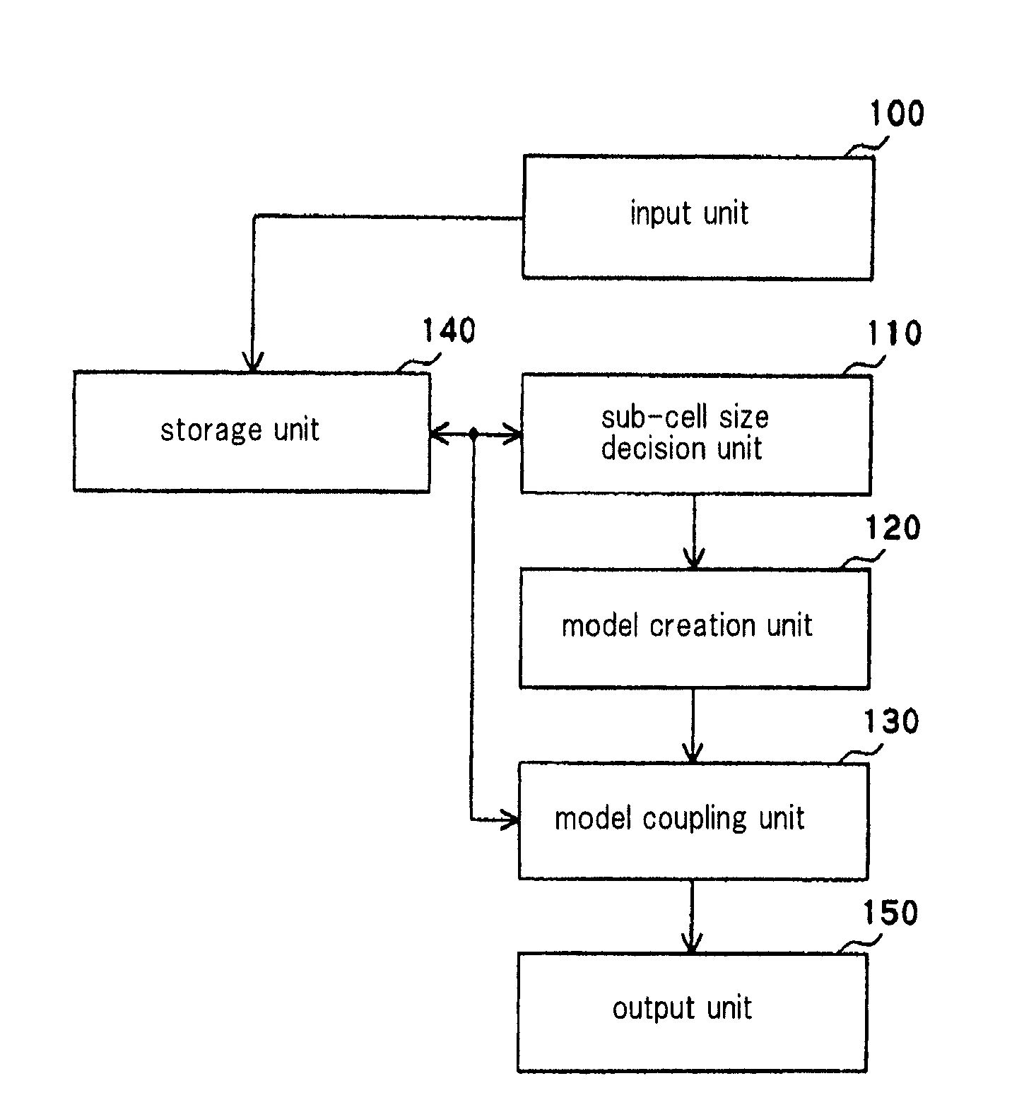
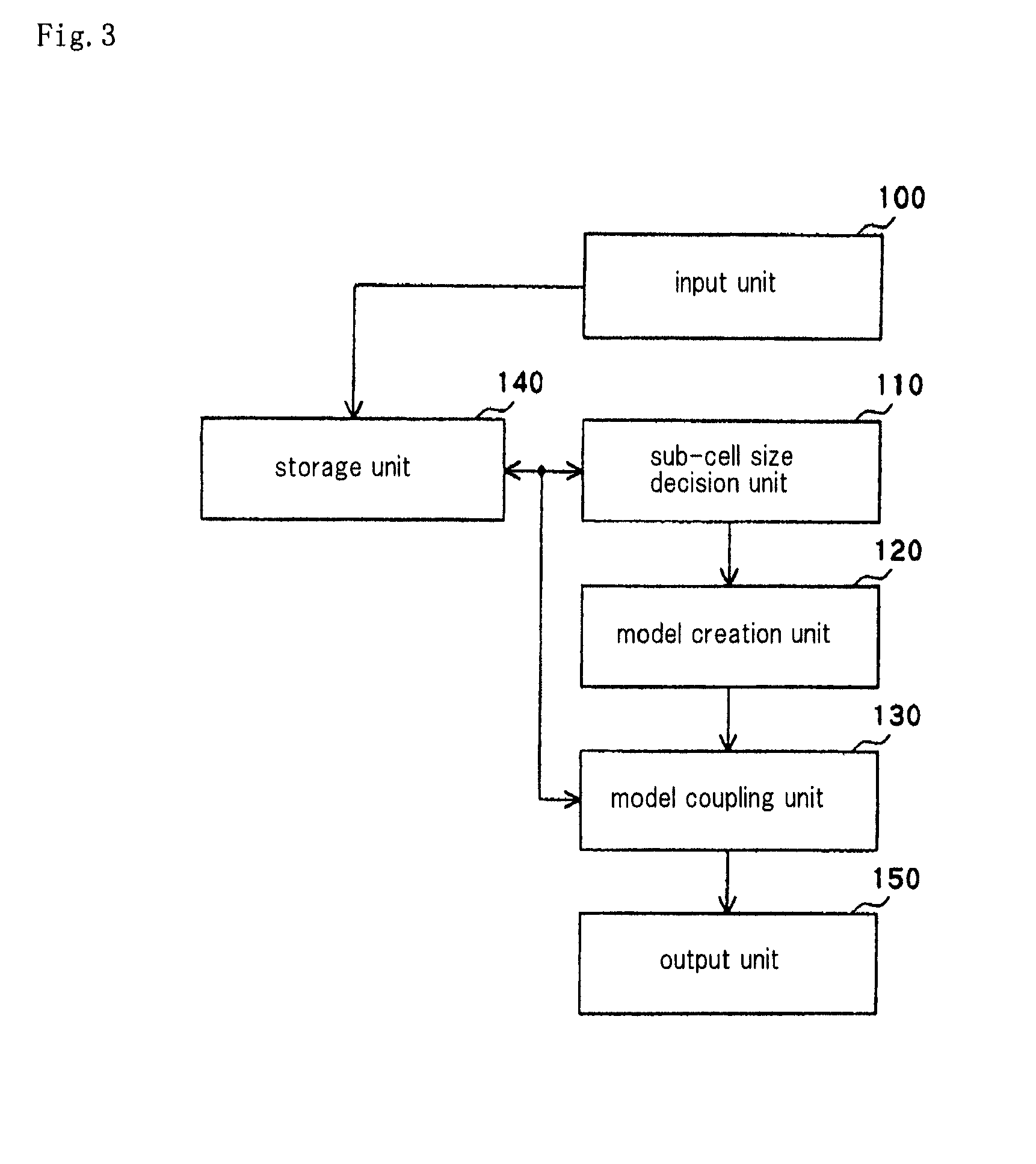
[0152]FIG. 3 is a diagram showing the configuration of a semiconductor integrated circuit power pin model creating apparatus of this embodiment. The apparatus comprises input unit 100 for entering data; divided cell size decision unit 110 for deciding the size of divided cells of an LSI; model creation unit 120 for creating a model of a power supply circuit network, a model of an active section, and a model of an internal capacitance section for each divided cell; model coupling unit 130 for coupling models for each cell to provide a power pin model of the LSI; storage unit 140 for stori...

second embodiment

[0188]In this embodiment, a description will be made of a method of creating a power pin model of a structure of an LSI having two power supply circuit network layers. In this case, an active section and an internal capacitance of the LSI exist between two types of power supply circuit network layers. Further, wires which constitute the power supply circuit network layers have respective capacitive components between them and ground. Here, the two power supply circuit network layers can be equivalently regarded as one power supply circuit network layer as shown in the first embodiment. In this case, a wiring capacitive component existing between the wire of the equivalent one power supply circuit network layer and ground is the total of the wiring capacitive components which exist between wires of the two power supply circuit network layers and ground. Accordingly, based on this idea, a power pin model of a structure having two power supply circuit network layers is created by the m...

third embodiment

[0223]In this embodiment, a description will be made of a method of creating a power pin model of an LSI in a case where there are a plurality of active sections and internal capacitance sections for the power pin model of the LSI in each cell.

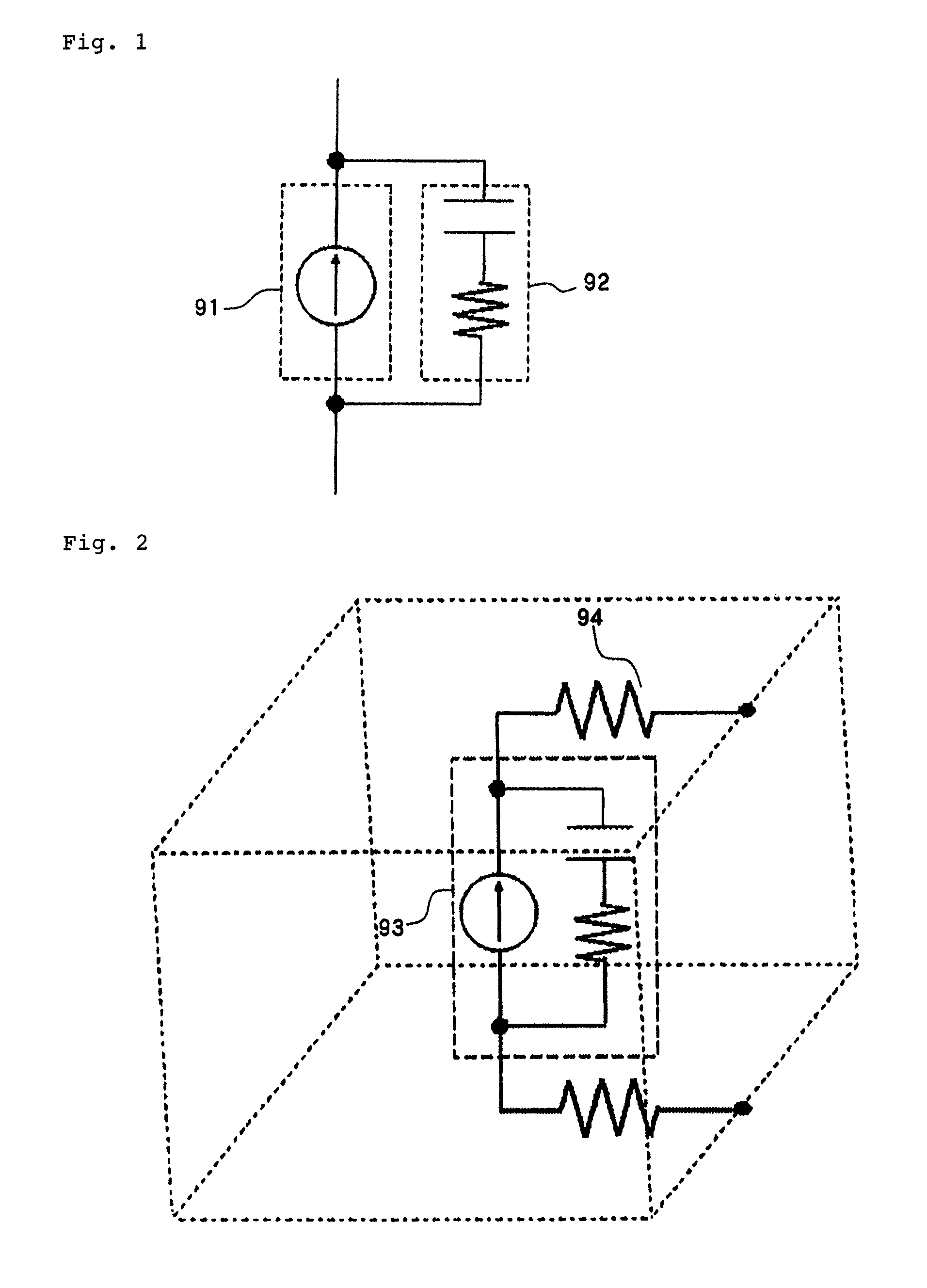
[0224]FIG. 12 shows, by way of example, a power pin model for an LSI having two power supply circuit network layers in the present embodiment, the power pin model having a power pin model in each cell which includes two types of active sections. Since there are two types of active sections which perform different operations, such as different operation frequencies of the LSI, two types of active sections 34a, 34b are created. Further, since there are two types of active sections in the model of the overall LSI in semiconductor integrated circuit entire power pin model 7 of input data in FIG. 9, each active section is distributed to each cell at an appropriate proportion based on the size of each cell determined by divided cell size decision un...


PUM


Abstract

A method of creating a power pin model of an LSI having appropriate analysis accuracy in consideration of information on positions within the LSI is provided. A divided cell size decision unit automatically decides a divided cell size of the LSI from power supply circuit network wire information, transistor structure information, analysis frequency information, size information, and element arrangement information of the LSI as well as from a semiconductor integrated circuit entire power pin model. A model creation unit allocates a model of an active section and a model of an internal capacitance section, including the positional information, within the LSI to the cells at an appropriate proportion, and a model coupling unit couples the models in each cell to create a power pin model of the LSI. Here, the size of each divided cell is determined to be electrically sufficiently smaller than a wavelength corresponding to an upper limit analysis frequency derived from power supply circuit network wire information, transistor structure information, and analysis frequency information.

Description

TECHNICAL FIELD[0001]The present invention relates to a method of creating a power pin model of a semiconductor integrated circuit, and more particularly, to a method, apparatus, and program for creating a power pin model which represents a change in a current which actually flows between power supply pins, in order to simulate a radiation electromagnetic field which is generated in a semiconductor integrated circuit.BACKGROUND ART[0002]EMI (Electromagnetic Interference: unwanted electromagnetic radiations) is generated from printed circuit boards (hereinafter also referred to as “PCB”) mounted in electronic devices. A main cause of the EMI generation may possibly be a high-frequency current on a PCB, particularly, a high-frequency current from a power supply pin of a semiconductor integrated circuit (Large Scale Integrated Circuit, hereinafter also referred to as “LSI”). Accordingly, as countermeasures to the EMI of electronic devices, a high-frequency current flowing through the p...

Claims


Application Information

Patent Timeline
Patent Type & Authority Patents(United States)
IPC IPC(8): G06F17/50
CPCG06F17/5036G06F30/367
Inventor OGAWA, MASASHIWABUKA, HIROSHI
Owner NEC CORP
Why Eureka
Try Eureka