
Lamb wave device

a technology of a beam wave and a beam wave, which is applied in the direction of piezoelectric/electrostrictive/magnetostrictive devices, piezoelectric/electrostriction/magnetostriction machines, impedence networks, etc., and can solve the problem that the influence of film thickness variations on resonant frequency variations cannot become an ignorable level

Active Publication Date: 2011-06-21
NGK INSULATORS LTD
View PDF10 Cites 44 Cited by
  • Summary
  • Abstract
  • Description
  • Claims
  • Application Information

AI Technical Summary

Benefits of technology

The present invention aims to provide a lamb wave device with small variations in frequency. The invention solves the problem of variations in frequency caused by variations in film thickness of the piezoelectric thin film and the pitch of the finger of the IDT electrode. The invention selects the film thickness and the pitch of the finger of the IDT electrode such that the sonic velocity of the lamb wave is not significantly affected by the film thickness. The invention also includes a support structure that isolates the excitation section of the laminate from the support substrate, suppressing etching of the piezoelectric thin film and further reducing variations in resonant frequency. Overall, the invention minimizes variations in frequency and improves the performance of the lamb wave device.

Problems solved by technology

However, also in International Publication No. 2007-046236, the influence exerted by variations in film thickness upon variations in resonant frequency does not become an ignorable level.

Method used


Image

  • Lamb wave device
  • Lamb wave device
  • Lamb wave device

Examples


first embodiment

1 First Embodiment

1-1 Configuration of Lamb Wave Device 102

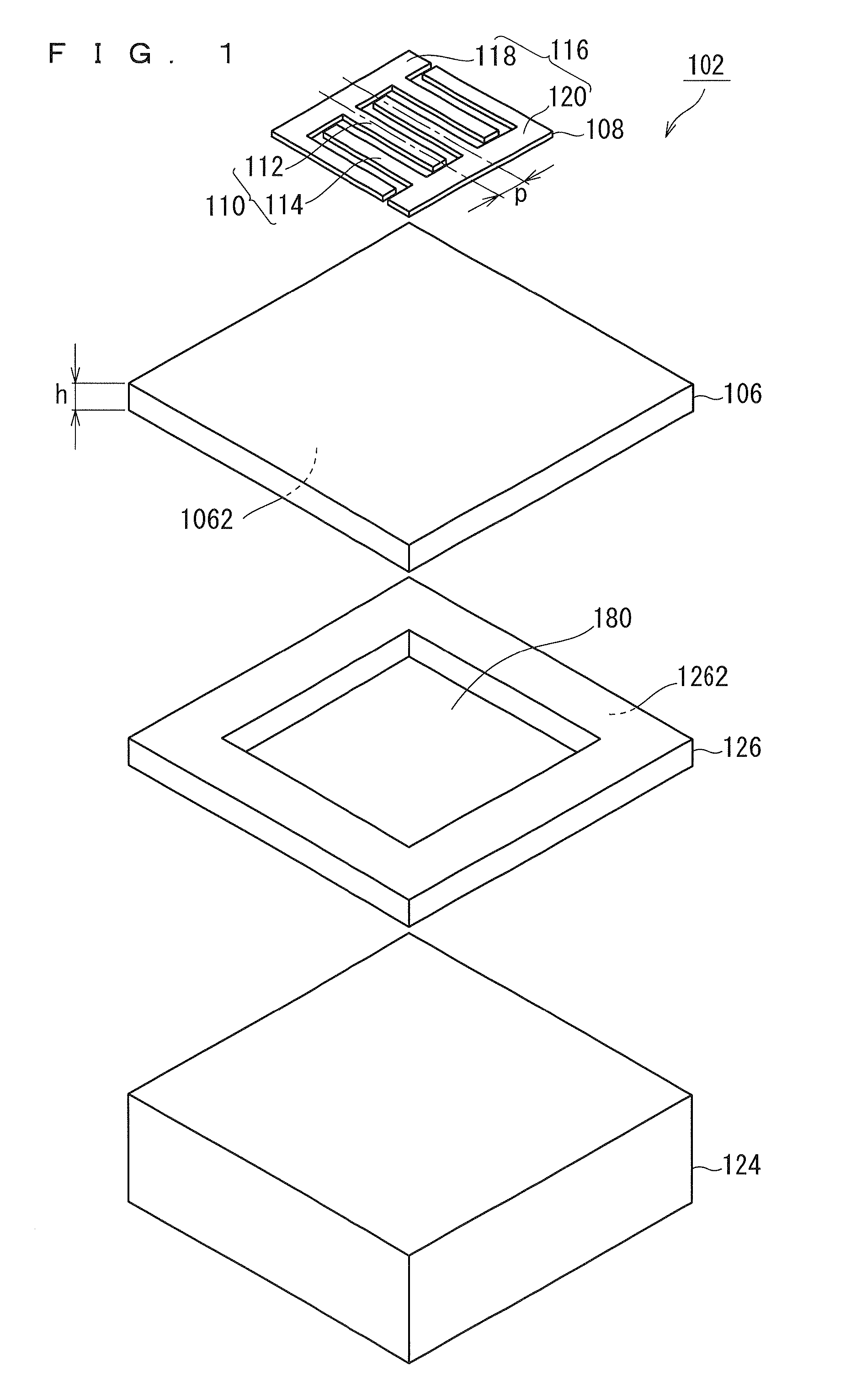
[0035]FIGS. 1 and 2 are schematic views of a lamb wave device 102 of a first embodiment. FIG. 1 is an exploded perspective view of the lamb wave device 102, and FIG. 2 is a sectional view of the lamb wave device 102.

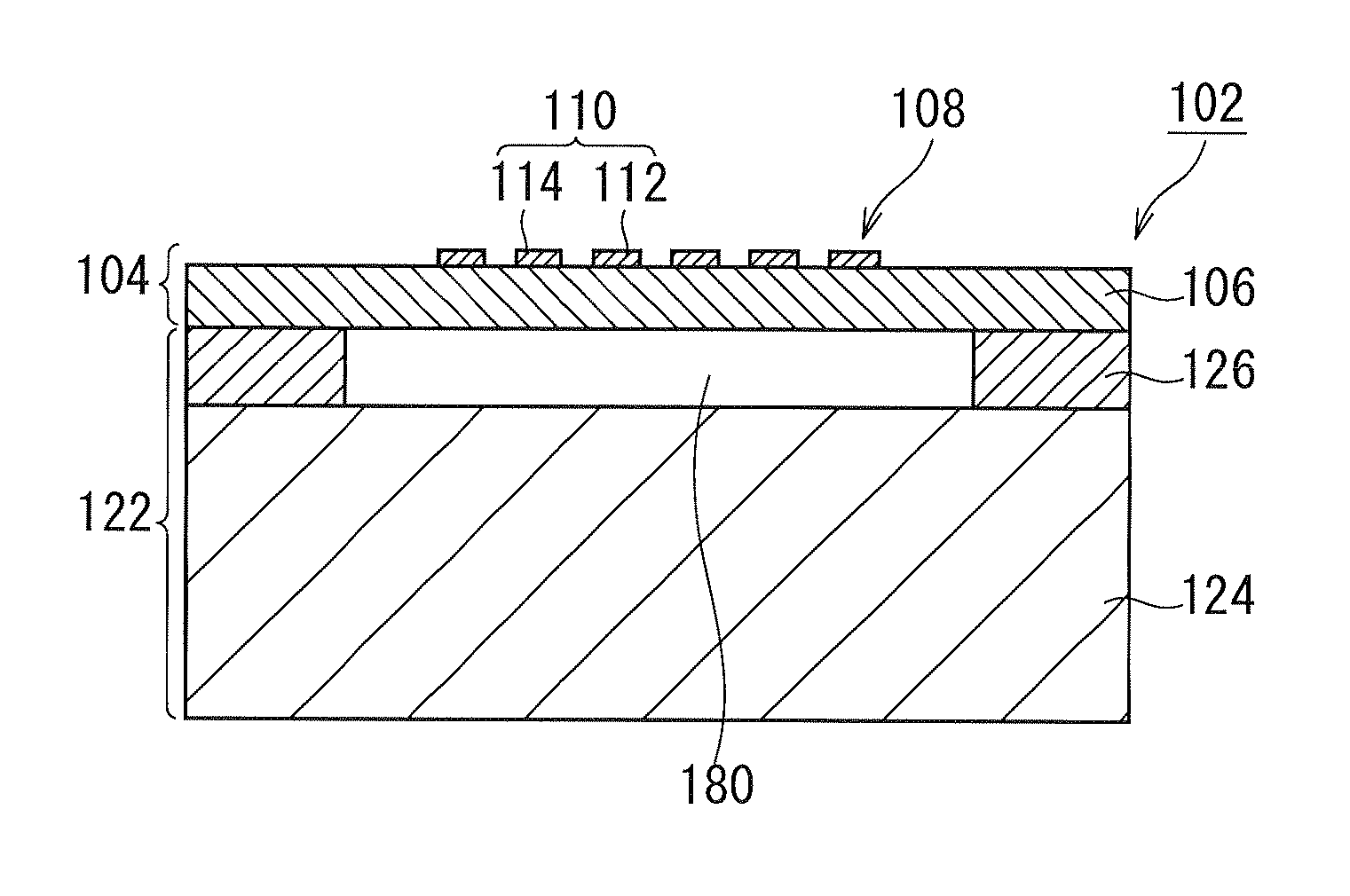
[0036]As shown in FIGS. 1 and 2, the lamb wave device 102 has a structure in which a support structure 122 supports a laminate 104. The laminate 104 is provided with a piezoelectric thin film 106 and an IDT electrode 108 that excites a lamb wave in the piezoelectric thin film 106. The support structure 122 is provided with a support substrate 124 and a support film 126 that bonds the support substrate 124 and the laminate 104. In the support film 126 formed is a cavity 180 that isolates an excitation section of the laminate 104 from the support substrate 124. The IDT electrode 108 is provided inside a region where the cavity 180 is formed (hereinafter referred to as a “cavity region”).

[0037]{Film Thickness h of P...

second embodiment

2 Second Embodiment

202>

[0071]A second embodiment relates to a lamb wave device 202 where, in place of the support structure 122 of the first embodiment, a support structure 222 supports a laminate 204 provided with a piezoelectric thin film 206 and an IDT electrode 208 in the same manner as in the first embodiment. FIG. 15 is a schematic view of the lamb wave device 202 of the second embodiment. FIG. 15 is a sectional view of the lamb wave device 202.

[0072]As shown in FIG. 15, the support structure 222 is provided with the support substrate 224, but is not provided with a support film. In the support substrate 224 formed is a cavity 280 for isolating an excitation section of the laminate 204 from the support substrate 224.

202>

[0073]FIGS. 16 to 18 are sectional views each explaining a manufacturing method for the lamb wave device 202. FIGS. 16 to 18 are sectional views of work-in-process products in the process of manufacturing.

[0074]{Production of Support Substrate 224}

[0075]In manu...

third embodiment

3 Third Embodiment

[0085]A third embodiment relates to a laminate 304 that can be adopted in place of the laminate 104 of the first embodiment, the laminate204 of the second embodiment and a laminate 504 of a fifth embodiment. FIG. 19 is a schematic view of the laminate 304 of the third embodiment. FIG. 19 is a sectional view of the laminate 304.

[0086]As shown in FIG. 19, the laminate 304 is provided with an IDT electrode 309 in addition to a piezoelectric thin film 306 and an IDT electrode 308 which are similar to the piezoelectric thin film 106 and the IDT electrode 108 of the first embodiment. The IDT electrode 309 is provided on the under surface of the piezoelectric thin film 306. The IDT electrode 309 has a similar plane shape to the IDT electrode 308, and is provided in a position opposed to the IDT electrode 308. A finger 310 of the opposed IDT electrode 308 and a finger 311 of the IDT electrode 309 have the same phase.

[0087]Also in the case of adopting such IDT electrodes 30...


PUM


Abstract

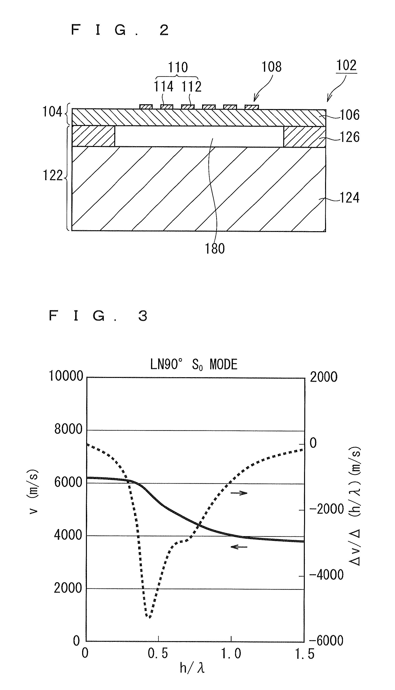
There is provided a lamb wave device with small variations in frequency, the device including: a piezoelectric thin film; an IDT electrode which is provided on a main surface of the piezoelectric thin film; and a support structure which supports a laminate of the IDT electrode and the piezoelectric thin film, and is formed with a cavity that isolates the laminate, wherein a film thickness h of the piezoelectric thin film and a pitch p of a finger of the IDT electrode are selected such that a lamb wave is excited at a target frequency, the lamb wave making dispersibility of a sonic velocity v with respect to the film thickness h of the piezoelectric thin film small.

Description

BACKGROUND OF THE INVENTION[0001]1. Field of the Invention[0002]The present invention relates to a lamb wave device which excites a lamb wave in a piezoelectric thin film.[0003]2. Description of the Background Art[0004]Japanese Patent Application Laid-Open No. 2007-228319 discloses a bulk acoustic wave device that excites thickness longitudinal vibration or thickness-shear vibration in a piezoelectric thin film obtained by removal processing on a piezoelectric substrate. In this bulk acoustic wave device, since a frequency is inversely proportional to a film thickness of the piezoelectric thin film, in order to make the frequency high, it is necessary to reduce the film thickness of the piezoelectric thin film. For example, in order to set the frequency to several GHz, it is necessary to set the film thickness of the piezoelectric thin film to approximately several μm depending upon a piezoelectric material constituting the piezoelectric thin film.[0005]However, when the film thickn...

Claims


Application Information

Patent Timeline
Patent Type & Authority Patents(United States)
IPC IPC(8): H01L41/08H10N30/00H10N30/80
CPCH03H9/02574H03H9/02228
Inventor TAI, TOMOYOSHISAKAI, MASAHIROOHSUGI, YUKIHISA
Owner NGK INSULATORS LTD
Learn More