Multi-layered device
a multi-layer device and multi-layer technology, applied in the direction of transformer/inductance details, printed inductances, basic electric elements, etc., can solve the problem of increasing the thickness of multi-layer devices, and achieve the effect of thinning the devi
- Summary
- Abstract
- Description
- Claims
- Application Information
AI Technical Summary
Benefits of technology
Problems solved by technology
Method used
Image
Examples
first embodiment
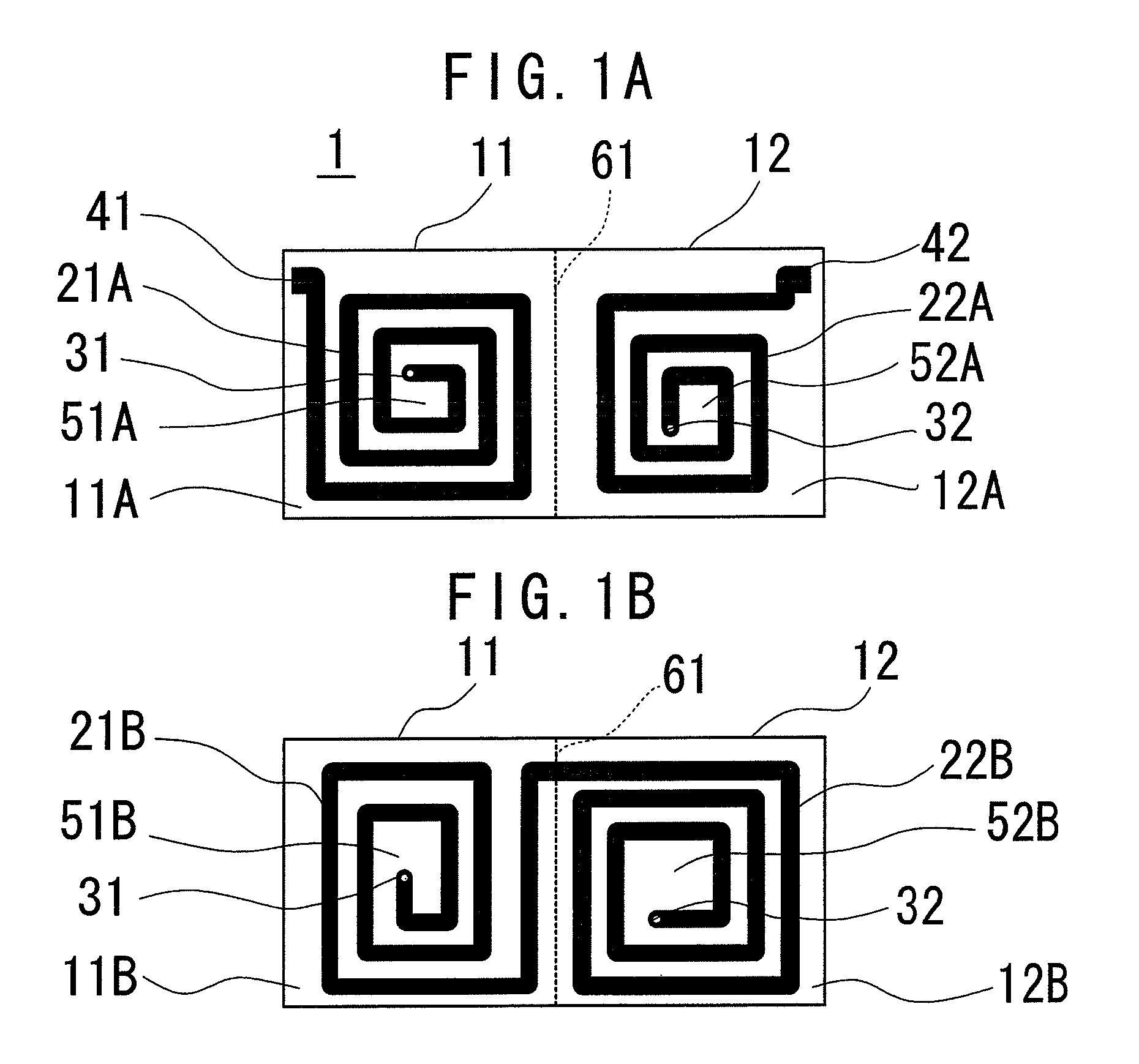
[0026]A multilayered device in accordance with a first embodiment of the present invention is described with reference to FIG. 1A and FIG. 1B. FIG. 1A shows a configuration of and patterns of conductors on a first face (front face) of an insulation sheet 1 which constitutes the multilayered device, and FIG. 1B shows a configuration of and patterns of conductors on a second face (rear face) thereof. Hereupon, the patterns of the conductors on the second face (rear face) shown in FIG. 1B are illustrated as patterns transparently observed from the same side of the patterns of the first face (front face). Therefore, when the patterns of the conductors on the second face (rear face) are observed from the second face side, the delineation will be reversed (the same goes for the following embodiments).
[0027]As shown in FIG. 1A and FIG. 1B, in the multilayered device in accordance with the first embodiment, the insulation sheet 1 has two foldable areas, that is, the first foldable area 11 a...
second embodiment
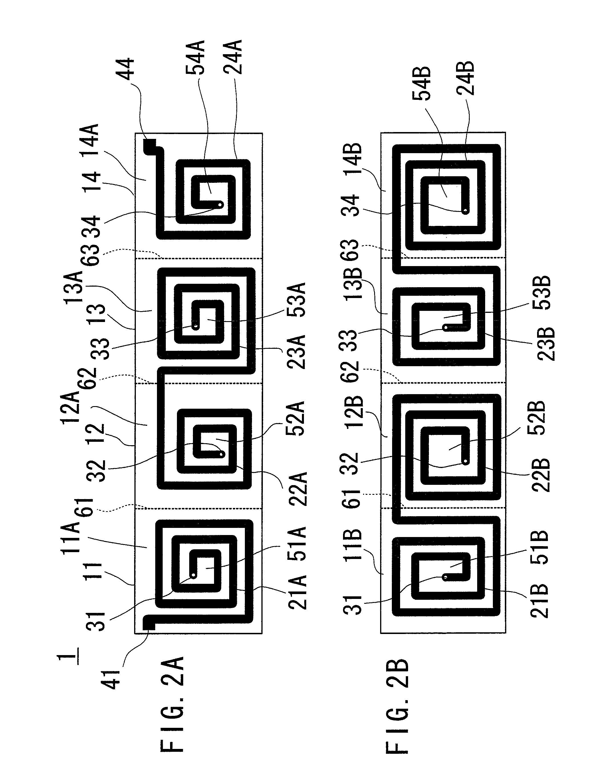
[0032]Subsequently, a multilayered device in accordance with a second embodiment of the present invention is described with reference to FIG. 2A and FIG. 2B. FIG. 2A shows a configuration of and patterns of conductors on a first face (front face) of an insulation sheet 1 which constitutes the multilayered device, and FIG. 2B shows a configuration of and patterns of conductors on a second face (rear face) thereof. Hereupon, the patterns of the conductors on the rear face shown in FIG. 2B are illustrated as patterns transparently observed from the same side of the patterns of the front face, similar to the above mentioned first embodiment. In addition, explanation of elements common in the above mentioned first embodiment are omitted (the same goes for the following embodiments).
[0033]In the second embodiment shown in FIG. 2A and FIG. 2B, an insulation sheet 1 is configured by four foldable areas 11 to 14. With respect to two foldable areas 11 and 12 adjoining each other, a foldable a...
third embodiment
[0037]Subsequently, a multilayered device in accordance with a third embodiment of the present invention is described with reference to FIG. 3A and FIG. 3B. FIG. 3A shows a configuration of and patterns of conductors on a first face (front face) of an insulation sheet 1 which constitutes the multilayered device, and FIG. 3B shows a configuration of and patterns of conductors on a second face (rear face) thereof. Hereupon, the patterns of the conductors on the rear face shown in FIG. 3B are illustrated as patterns transparently observed from the same side of the patterns of the front face, similar to the above mentioned first embodiment.
[0038]The multilayered device in accordance with the third embodiment is configured as a transformer having two windings. An insulation sheet 1 has two foldable areas, that is, a first foldable area 11 and a second foldable area 12, which are to be multilayered by being folded. First conductors 21A and 22A, which constitute first coils 51A and 52A eac...
PUM
| Property | Measurement | Unit |
|---|---|---|
| areas | aaaaa | aaaaa |
| area | aaaaa | aaaaa |
| foldable area | aaaaa | aaaaa |
Abstract
Description
Claims
Application Information


