

Power layout of integrated circuits and designing method thereof
a technology of integrated circuits and layouts, applied in the direction of software simulation/interpretation/emulation, instruments, program control, etc., can solve the problems of imposing a huge human resource burden, and achieve the effect of reducing the impedance difference between facilitating routing congestion of the power mesh and the power supply ring, and facilitating effective elimination of the burden of human resources
- Summary
- Abstract
- Description
- Claims
- Application Information
AI Technical Summary
Benefits of technology
Problems solved by technology
Method used
Image

Examples
Embodiment Construction
[0021]The characteristic, spirit, advantage, and convenience in practice of the invention can be particularly explained by the following preferred embodiments according to the invention.
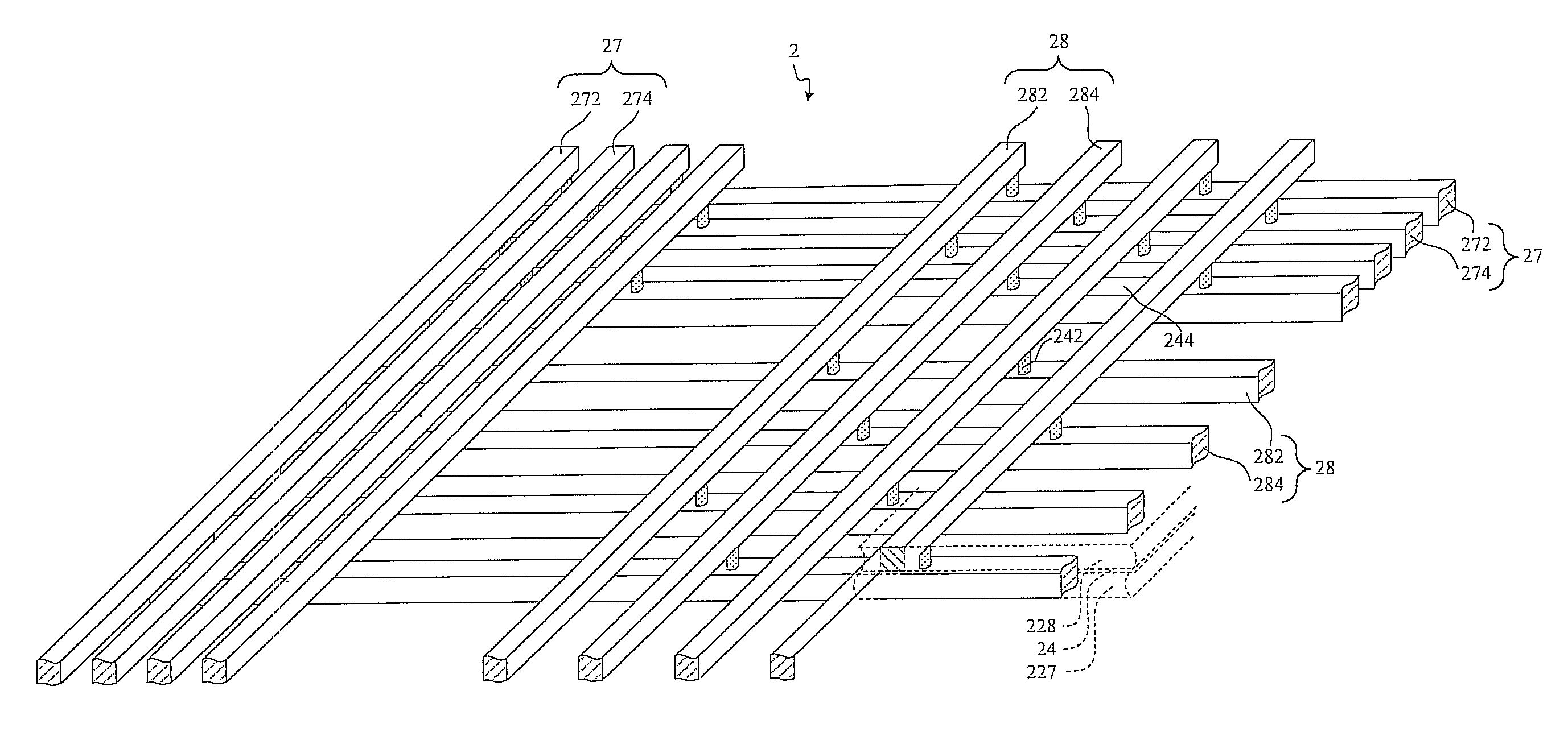
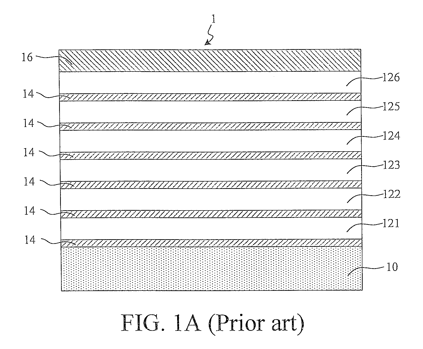
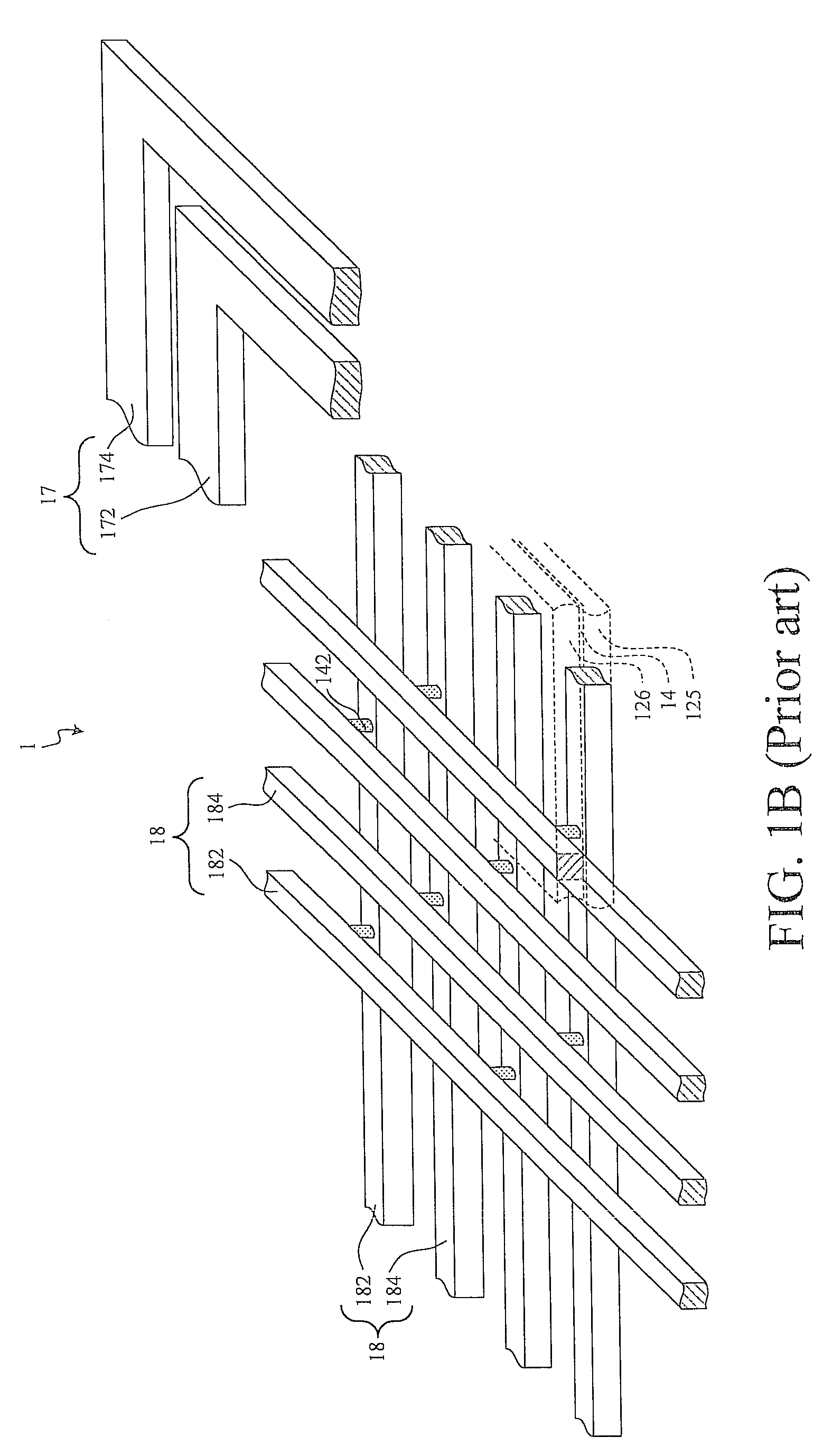
[0022]Please refer to FIG. 2A. FIG. 2A shows a simplified sectional view of an IC die (or a chip) 2 in a preferred embodiment according to the invention. As shown in FIG. 2A, the IC die 2 includes a semiconductor layer 20, eight successive metal layers (221˜228) from bottom to top, several insulating layers 24 formed between two adjacent metal layers respectively, and a passivation layer 26. The semiconductor layer 20 is used for forming electronic components such as transistors (not shown in FIG. 2A). The number of the metal layers is determined by the complexity of the practical routing. Thus, the eight metal layers shown in FIG. 2A are provided only for the convenience of explanation, not as a limit to the invention.
[0023]Regarding the routing at the metal layers 221˜228, a power distribution netw...
PUM
 Abstract
Description
Claims
Application Information