Phase shifter having switchable high pass filter and low pass filter paths and impedance adjustment circuits

a phase shifter and low-pass filter technology, applied in the field of filter switching type phase shifters, can solve the problems of signal insertion loss, worsening reflection loss, and impedance difference needs to be ameliorated, so as to reduce the effect of insertion loss and diminish the effect of manufacture tolerances

Inactive Publication Date: 2007-07-03
RENESAS ELECTRONICS CORP
View PDF6 Cites 36 Cited by
  • Summary
  • Abstract
  • Description
  • Claims
  • Application Information

AI Technical Summary

Benefits of technology

[0016]That is, except the case of the values of components for specified phase shift values, such as 180°, the impedance value after current passage through the high-pass filter differs from that after current passage through the low-pass filter, under the effect of reactance components, if any, in the impedances on the input / output sides of the filter. This difference in impedance needs to be ameliorated because it may give rise to signal insertion loss difference, variations in the phase shift value caused by a mismatch between the load impedance and the filter units, insertion loss at the time of switching between the filter units, and to worsened reflection losses.
[0017]Meanwhile, with the phase shifter disclosed in Patent Document 1, matching resistors are inserted on the input and output sides of the switch means to cancel out the reflection caused by impedance mismatch. This phase shifter has, however, a drawback that, since resistance matching circuits are provided forward and in rear of the switches, the number of circuits added is increased, and hence the component area occupied becomes broader, thus raising the chip cost. Moreover, since the resistance matching circuit includes an internal resistance connected in parallel with the signal transmitting channel, part of the signal is consumed in this matching resistor, thus raising insertion losses. In particular, since matching resistors are connected to the input and output sides of the switch means, the loss by the matching resistor is increased significantly when a plural number of the phase shifters are arranged in plural stages.
[0019]Therefore there is much to be desired in the art for a phase shifter with a reduced insertion loss, in which the impedance mismatch after passage of the current through the high-pass filter or low-pass filter as well as the difference in insertion losses between the high-pass filter and the low-pass filter, or the phase shifting error, may be diminished.
[0020]According to the present invention, the following principle is proposed. That is, a circuit, composed of a capacitor and an inductor, such that will cancel out the reactance component of the impedance produced in a single pole double throw switch, to a single pole side of the switch, to change the impedance at the sites of insertion of filter units, to eliminate the impedance mismatch at a site downstream of the filter units in the signal flow direction.

Problems solved by technology

This difference in impedance needs to be ameliorated because it may give rise to signal insertion loss difference, variations in the phase shift value caused by a mismatch between the load impedance and the filter units, insertion loss at the time of switching between the filter units, and to worsened reflection losses.

Method used


Image

  • Phase shifter having switchable high pass filter and low pass filter paths and impedance adjustment circuits
  • Phase shifter having switchable high pass filter and low pass filter paths and impedance adjustment circuits
  • Phase shifter having switchable high pass filter and low pass filter paths and impedance adjustment circuits

Examples


first embodiment

[First Embodiment]

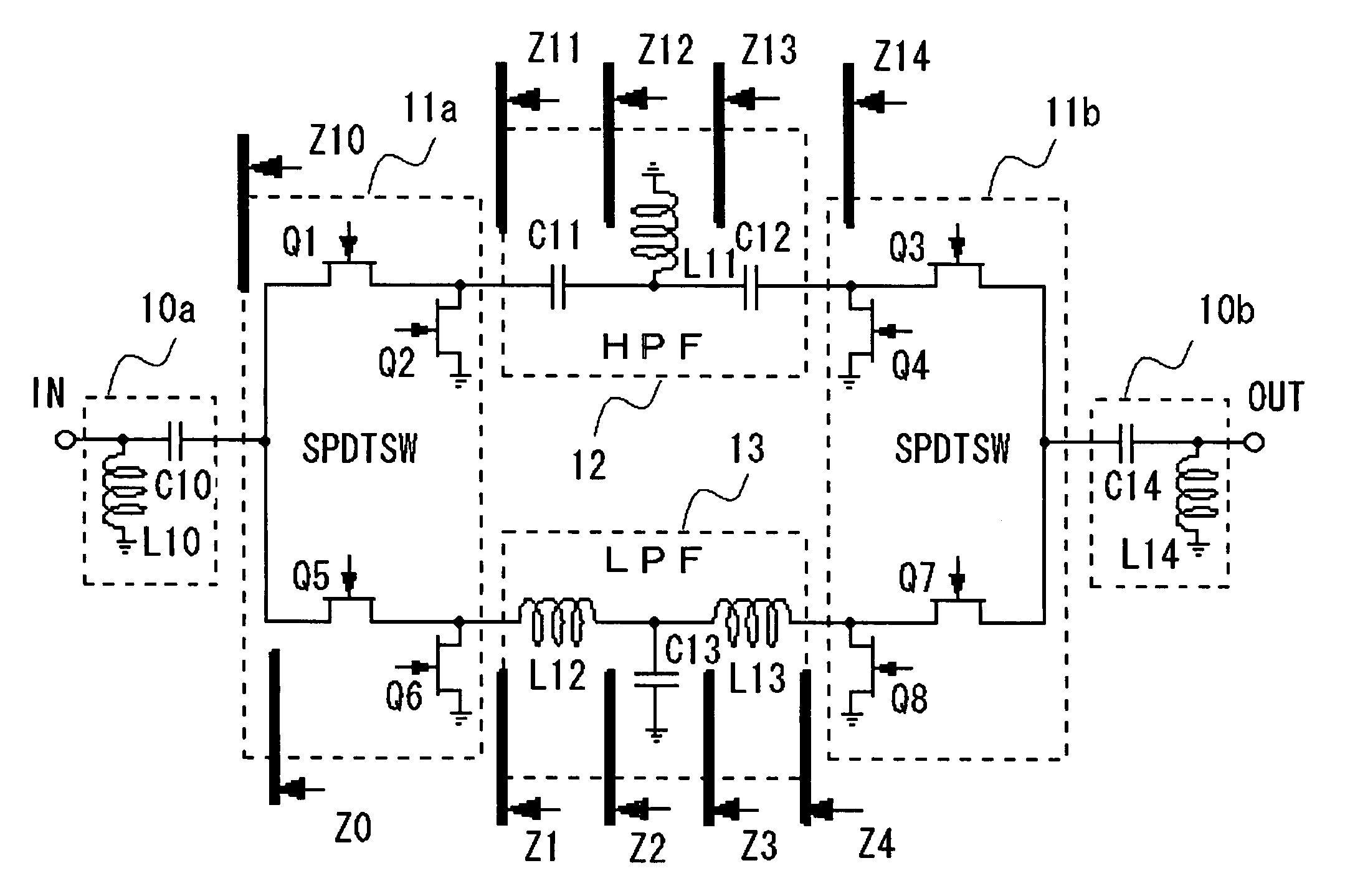
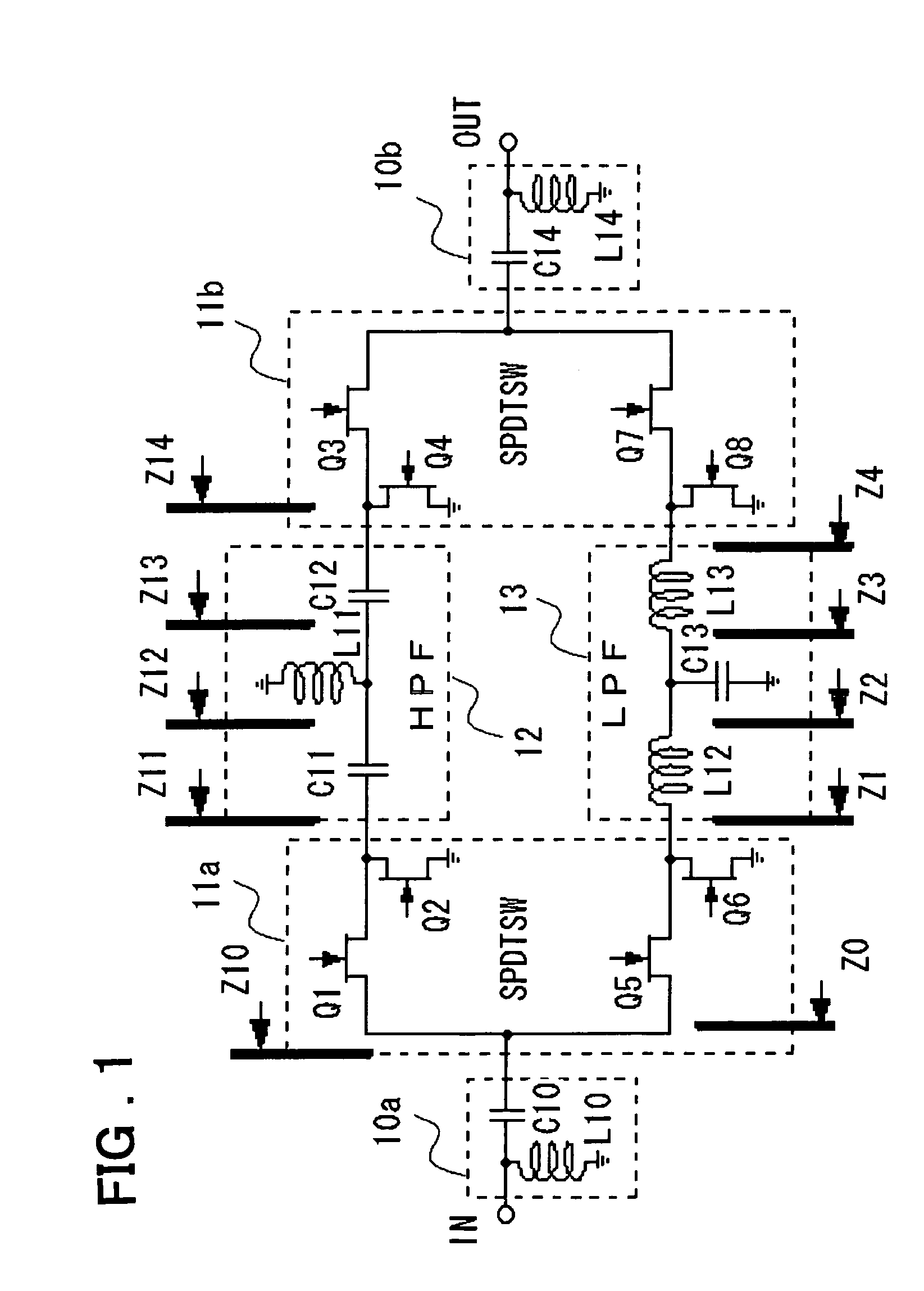
[0039]FIG. 1 is a circuit diagram showing the configuration of a phase shifter according to a first embodiment of the present invention. In FIG. 1, the phase shifter includes impedance adjustment circuits 10a, 10b, single pole double throw switches 11a, 11b, a high-pass filter 12 and a low-pass filter 13.

[0040]The impedance adjustment circuit 10a is made up by an inductor L10, connected across an input terminal IN and the ground, and a capacitor C10, connected across the input terminal IN and the single pole double throw switch 11a. Similarly, the impedance adjustment circuit 10b is made up by an inductor L14, connected across an output terminal OUT and the ground, and a capacitor C14, connected across the output terminal OUT and the single pole double throw switch 11b.

[0041]The single pole double throw switch ha is made up by a FET Q1, connected across a single pole side, connected to the impedance adjustment circuit 10a, and the high-pass filter 12, a VET Q2, co...

second embodiment

[Second Embodiment]

[0059]FIG. 3 depicts a circuit diagram showing the structure of a phase shifter according to a second embodiment of the present invention. In FIG. 3, the same reference numerals and labels are used to depict the same components. What makes FIG. 3 significantly different from FIG. 1 is that inductors L21, L23, L22 and L24 are connected across the sources and the drains of the FETs Q1, Q3, Q5 and Q7 in the single pole double throw switches 11c, 11d, respectively. Such parallel connection of the FET and the inductor forms a switch exploiting the resonance between the inductor and the parasitic capacitance of the FET. That is, in the present second embodiment, a resonance switch composed of an inductor and an FET, to the source and drain of which the inductor is connected in parallel, is substituted for each of the single pole double throw switches 11c, 11d.

[0060]The operation of the phase shifter, shown in FIG. 3, is that, when signals are passed through the high-pa...


PUM


Abstract

A phase shifter with a low insertion loss in which impedance mismatch at a point in rear of a high-pass filter or a low-pass filter in the signal flow direction is reduced and difference in insertion loss or phase shifting error across a high-pass filter- low-pass filter is suppressed. A single pole double throw switch, provided on the input side, and another single pole double throw switch, provided on the output side and operatively linked to the single pole double throw switch, are changed over between a low-pass filter and a high-pass filter. An impedance adjustment circuit, provided between an input terminal and the single pole double throw switch, is made up by a capacitor, connected across the input terminal and a single pole side junction of the single pole double throw switch, and an inductor connected across the input terminal and ground.

Description

FIELD OF THE INVENTION[0001]This invention relates to a phase shifter and, more particularly, to a filter switching type phase shifter for use in the integrated circuits, generally.BACKGROUND OF THE INVENTION[0002]The filter switching type phase shifter is usually made up by a high-pass filter (HPF) for producing the phase lead of the signal phase, a lowpass filter (LPF) for producing the phase lag of the signal phase and single pole double throw switches (SPDT switches) for switching between the high-pass and low-pass filters. The quantity of phase shift is created by the phase difference produced on switching between these two filters.[0003]The configuration of this filter switching type phase shifter will now be explained. FIG. 4 depicts a circuit diagram of a state-of-the-art filter switching type phase shifter. A high-pass filter (HPF) 102 is made up by two capacitors C101, C102, connected in series with a signal line, and an inductor L101, connected from a junction of the two ...

Claims


Application Information

Patent Timeline
Patent Type & Authority Patents(United States)
IPC IPC(8): H01P1/18
CPCH03H7/20H03H9/66
Inventor NAKAMURA, JUNICHI
Owner RENESAS ELECTRONICS CORP
Why Eureka
Try Eureka