Organic electroluminescent device, method for producing organic electroluminescent device, and electronic apparatus

a technology of electroluminescent devices and organic materials, which is applied in the manufacture of electrode systems, electric discharge tubes/lamps, and discharge tubes luminescent screens, etc., can solve the problems of difficult design of optical systems that control light emanating from organic light-emitting layers, and difficult top-emission structures to use. achieve the effect of low non-uniformity of luminance and high luminan

Inactive Publication Date: 2011-07-05
138 EAST LCD ADVANCEMENTS LTD
View PDF3 Cites 0 Cited by
  • Summary
  • Abstract
  • Description
  • Claims
  • Application Information

AI Technical Summary

Benefits of technology

[0008]In this case, at least part of the second electrode is covered with the protective layer or the third electrode. Thus, a region of the second electrode covered with the protective layer or the third electrode can be protected from an etching atmosphere in etching the organic light-emitting layer. That is, the at least part of the second electrode can be protected from damage due to the etching; hence, the second electrode can have a uniform thickness in this region. Thus, a uniform current can flow through the organic light-emitting layer compared with the case where the protective layer is not formed, thereby suppressing nonuniformity in luminance.
[0039]In this case, the electronic apparatus includes any one of the organic electroluminescent devices described above; hence, the electronic apparatus can have high luminance and low nonuniformity in luminance compared with the related art.

Problems solved by technology

The use of the electrode having a large thickness reduces light transmittance, so that it is difficult to use a top-emission structure.
In the case of using the bottom-emission structure, light radiates from the substrate having a thickness of about 0.5 mm, thus disadvantageously leading to difficulty in designing an optical system that controls light emanating from the organic light-emitting layer.

Method used


Image

  • Organic electroluminescent device, method for producing organic electroluminescent device, and electronic apparatus
  • Organic electroluminescent device, method for producing organic electroluminescent device, and electronic apparatus
  • Organic electroluminescent device, method for producing organic electroluminescent device, and electronic apparatus

Examples


first embodiment

Organic Electroluminescent Element and Electronic Apparatus Including Same

[0055]Embodiments of the invention will be described below with reference to the attached drawings.

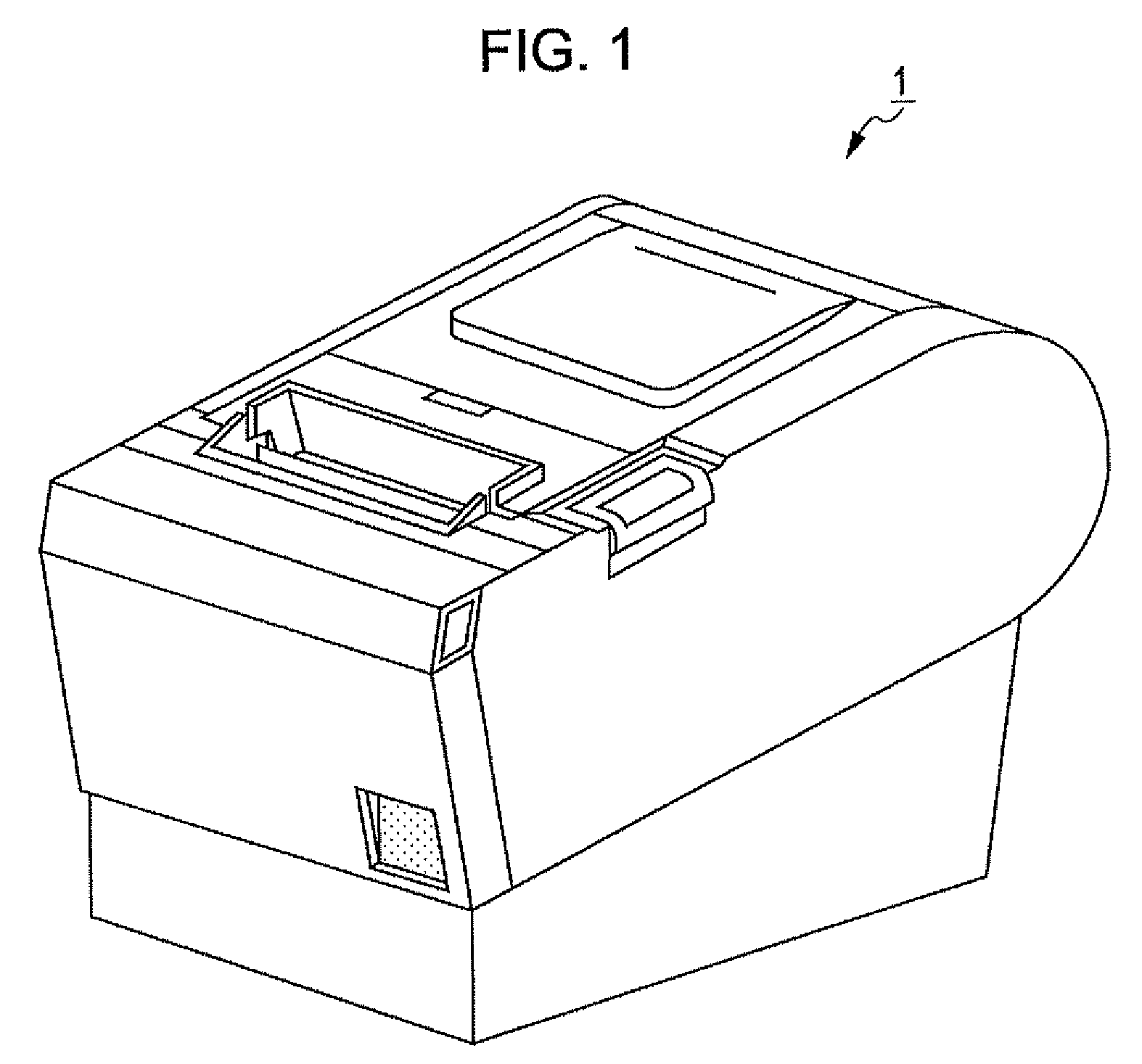
[0056]FIG. 1 is a perspective view of a page printer serving as an electronic apparatus. A page printer 1 feeds in a print sheet in a feed tray, performs printing processing, and outputs the print sheet with image information.

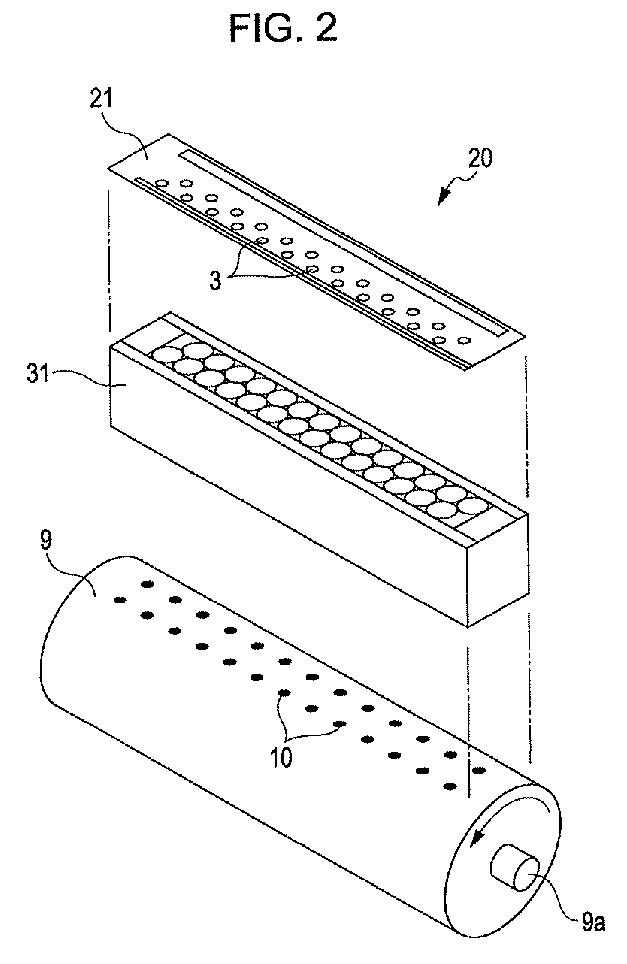
[0057]FIG. 2 is a schematic view of an exposure unit 20 arranged in the page printer 1 according to an embodiment. The exposure unit 20 includes a line head 21 constituted by organic electroluminescent elements (hereinafter, referred to as “organic EL elements”) 3, a lens array 31 configured to bring light passing through the line head 21 into focus to form an image, a photoconductive drum 9 exposed with light passing through the lens array 31 from the line head 21, and a rotating drum shaft 9a.

[0058]When the organic EL elements 3 emit light beams, the photoconductive drum 9 is irradiated w...

second embodiment

Method for Producing Organic EL Element

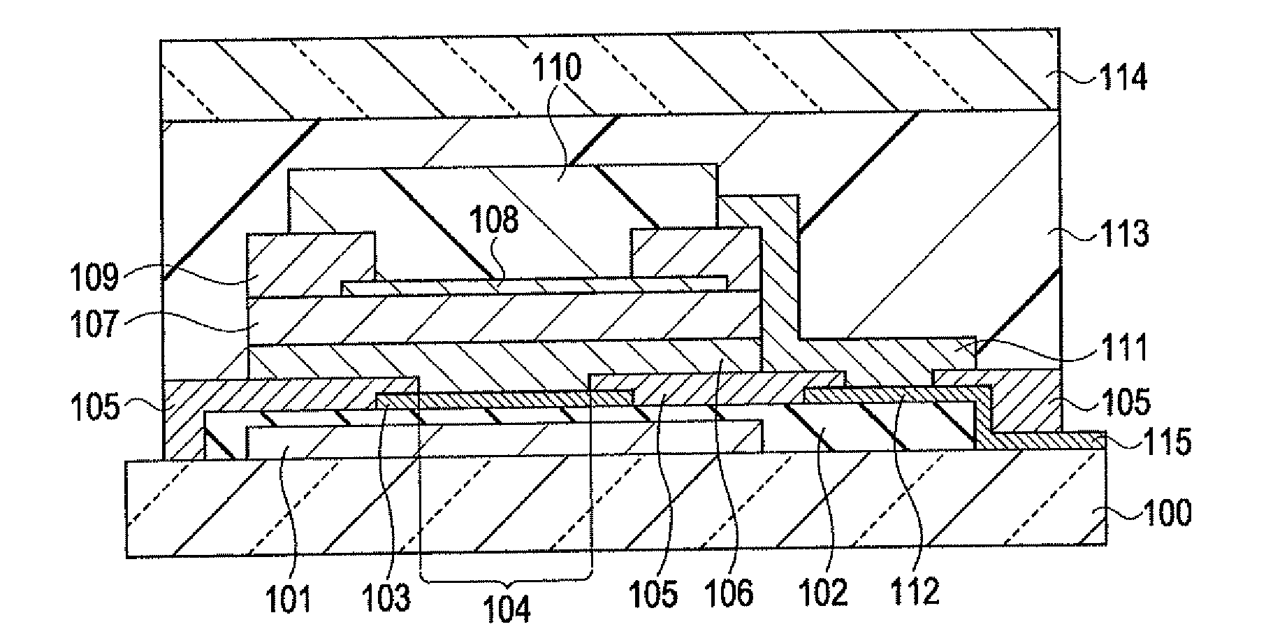
[0086]A method for producing an organic EL element will be described below with reference to the attached drawings. FIGS. 4A, 4B, and 5 are cross-sectional views illustrating a procedure for producing the organic EL element 3.

[0087]As a step 1, after the optically transparent substrate 100 composed of, for example, glass is rinsed, an aluminum layer having a thickness of, for example, about 200 nm is deposited thereon by, for example, evaporation. An unnecessary portion is removed by photolithography and etching to form the reflective layer 101. Alternatively, in this step, the reflective layer 101 may be formed by evaporation with a shadow mask.

[0088]As a step 2, silicon nitride is deposited thereon by, for example, chemical vapor deposition (CVD). An unnecessary portion is removed by photolithography and etching to form the interlayer insulating layer 102. The arrangement of the interlayer insulating layer 102 prevents electrolytic corrosion ...

first modification

of Second Embodiment

[0100]In the foregoing embodiment, the reflective layer 101, the interlayer insulating layer 102, and the positive electrode 103 are formed on the substrate 100 by the steps 1 to 3. Alternatively, the reflective layer 101, the interlayer insulating layer 102, and the positive electrode 103 may be replaced with a light-reflective positive electrode 103, simplifying the production process. In this case, the positive electrode 103 is composed of a material selected from silver, gold, nickel, palladium, platinum, silicon, alloys thereof, mixtures thereof, and doped materials thereof and has a thickness of about 200 nm. The light-reflective positive electrode can be formed by, for example, evaporation with a shadow mask.

[0101]The shape of the current-carrying portion 104 formed in the step 4 is not limited to a circle having a diameter of about 40 μm. Examples of the shape of the current-carrying portion 104 that may be used include rectangles, ellipses, polygons, ind...


PUM


Abstract

A method for producing an organic electroluminescent device includes forming a first electrode configured to partially cover a substrate, forming an organic light-emitting layer configured to cover the first electrode, forming an optically transparent second electrode that lies on a side of the organic light-emitting layer opposite the side adjacent to the first electrode and is superposed on a current-carrying portion of the first electrode in plan, forming a third electrode in at least part of a region that is not superposed on the current-carrying portion in plan, the third electrode being electrically connected to part of the second electrode, forming an optically transparent protective layer configured to cover at least a region of the second electrode where the second electrode is not superposed on the third electrode in plan, and removing part of the organic light-emitting layer with the third electrode and the protective layer serving as a mask.

Description

BACKGROUND[0001]1. Technical Field[0002]The present invention relates to an organic electroluminescent device, a method for producing an organic electroluminescent device, and an electronic apparatus.[0003]2. Related Art[0004]Organic electroluminescent elements have been applied to light sources of printers. When organic electroluminescent elements are used as light sources of printers, it is important that the organic electroluminescent elements should emit highly uniform monochromatic light. As a method for forming organic electroluminescent elements with high uniformity, a method has been known in which an organic-light-emitting-layer precursor is applied to the entire surface of a substrate by, for example, spin coating, followed by drying and annealing, and then an unnecessary portion is removed by etching. JP-A-2007-242436 discloses a method including etching an organic light-emitting layer with a second electrode (which cooperates with a first electrode located adjacent to a ...

Claims


Application Information

Patent Timeline
Patent Type & Authority Patents(United States)
IPC IPC(8): H01J9/24
CPCB41J2/45H01L51/5203H01L51/56H01L27/3297H01L51/5237H01L2251/5315H10K59/179H10K59/1795H10K50/805H10K50/856H10K50/844H10K50/8426H10K2102/3026H10K71/00
Inventor UCHIDA, MASAHIROKIMURA, HIDEYUKI
Owner 138 EAST LCD ADVANCEMENTS LTD
Why Eureka
Try Eureka