Field-effect transistor having group III nitride electrode structure

a field-effect transistor and electrode structure technology, applied in the field of field-effect transistors, can solve problems such as new problems that are not conventionally known, and achieve the effect of facilitating formation and allowing a large improvement of output properties

Inactive Publication Date: 2011-07-05
NEC CORP
View PDF20 Cites 33 Cited by
  • Summary
  • Abstract
  • Description
  • Claims
  • Application Information

AI Technical Summary

Benefits of technology

[0029]In view of the foregoing, an object of the invention is to provide a transistor which is excellent for the balance between the collapse and the gate breakdown voltage. Another object of the invention is to provide a transistor which is excellent for the reliability and high-frequency properties in addition to the performance balance between the collapse and the gate breakdown voltage.
[0053]As described above, in the field-effect transistor of the invention, the suppression of the collapse and the higher gate breakdown voltage can simultaneously be realized. Accordingly, the output properties can be largely improved during the large signal operation with the high voltage.

Problems solved by technology

However, in the case where the structure described in Non-Patent Reference 3 is adopted, as a result of study of the inventor, it is found that the new problem which is not conventionally known is generated.

Method used


Image

  • Field-effect transistor having group III nitride electrode structure
  • Field-effect transistor having group III nitride electrode structure
  • Field-effect transistor having group III nitride electrode structure

Examples


example 1

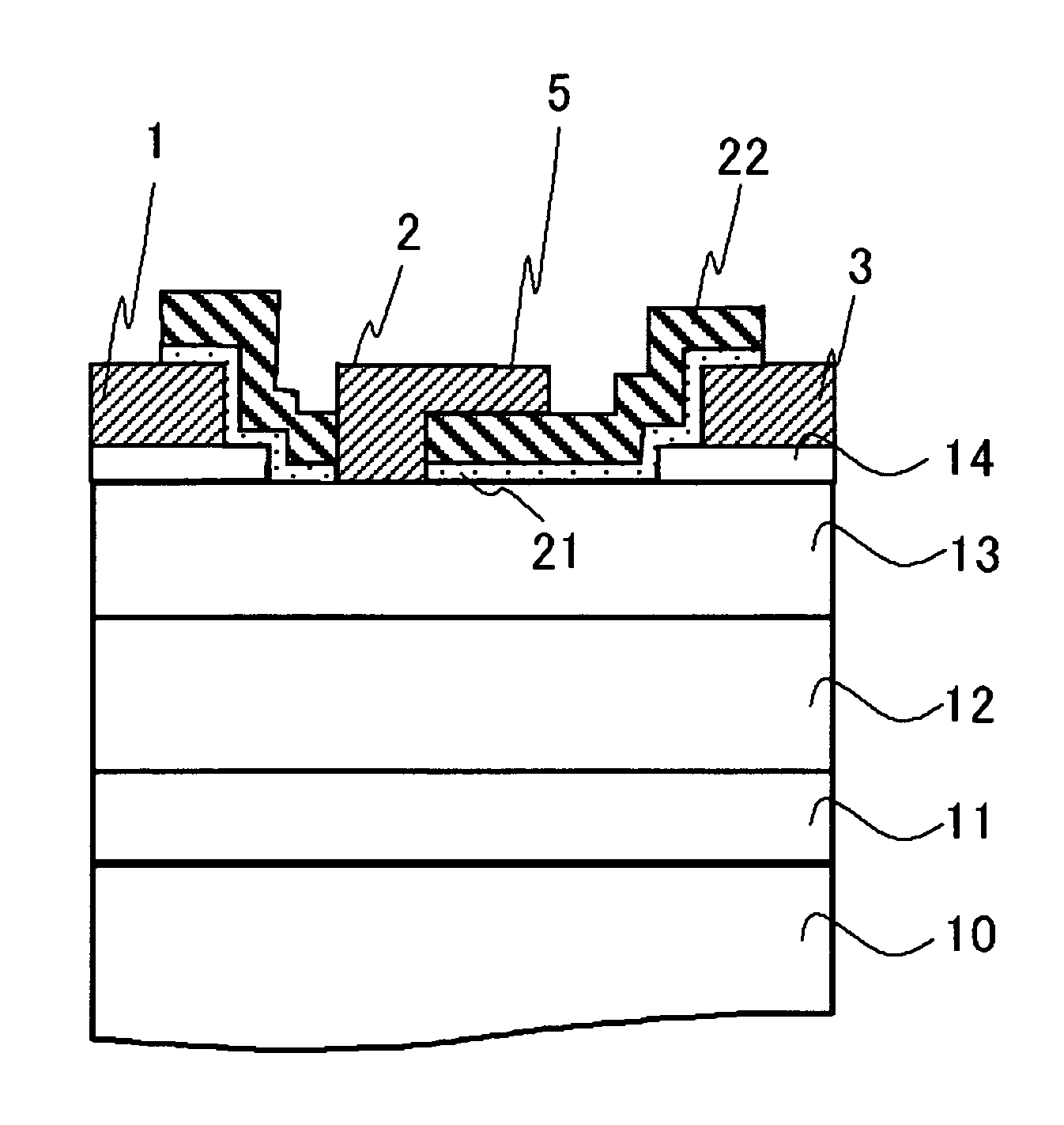
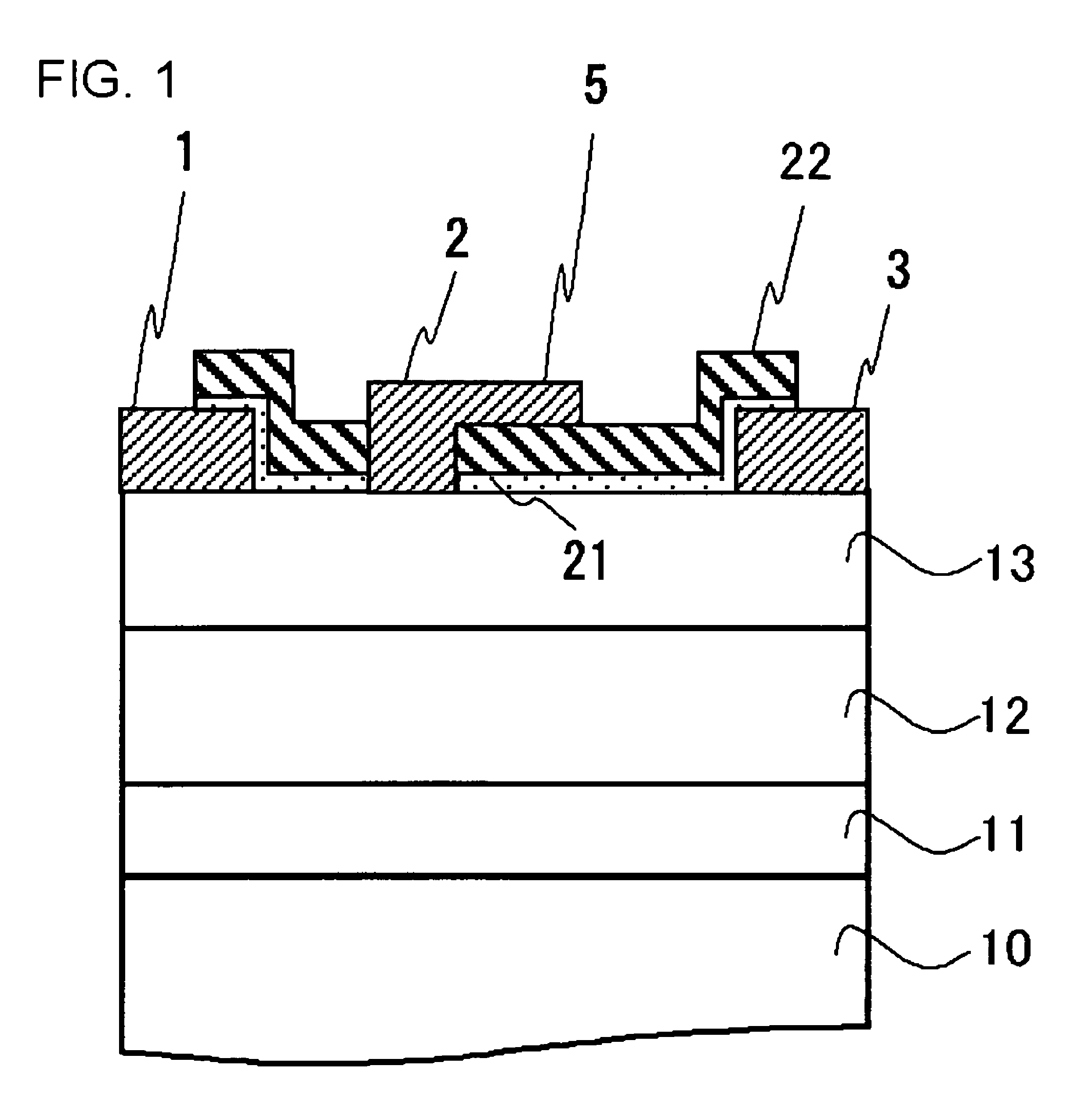
[0095]FIG. 1 shows a sectional structure of HJFET in Example 1. HJFET is formed on a substrate 10 made of a material such as SiC. A buffer layer 11 including a semiconductor layer is formed on the substrate 10. A GaN channel layer 12 (abbreviated as “GaN channel 12” in FIG. 1, hereinafter referred to as “GaN channel 12” in the following drawings) is formed on the buffer layer 11. An AlGaN electron supply layer 13 is formed on the GaN channel layer 12. A source electrode 1 and a drain electrode 3, in which ohmic contact is secured, are formed on the electron supply layer. A gate electrode 2, in which Schottky contact is secured, is provided between the source electrode 1 and the drain electrode 3. The gate electrode 2 has a field plate portion 5 overhanging the drain side in a visored shape. A surface of the electron supply layer 13 is covered with a SiN film 21, and a SiO2 film 22 is further provided on the SiN film 21. The SiN film 21 and the SiO2 film 22 are provided immediately b...

example 2

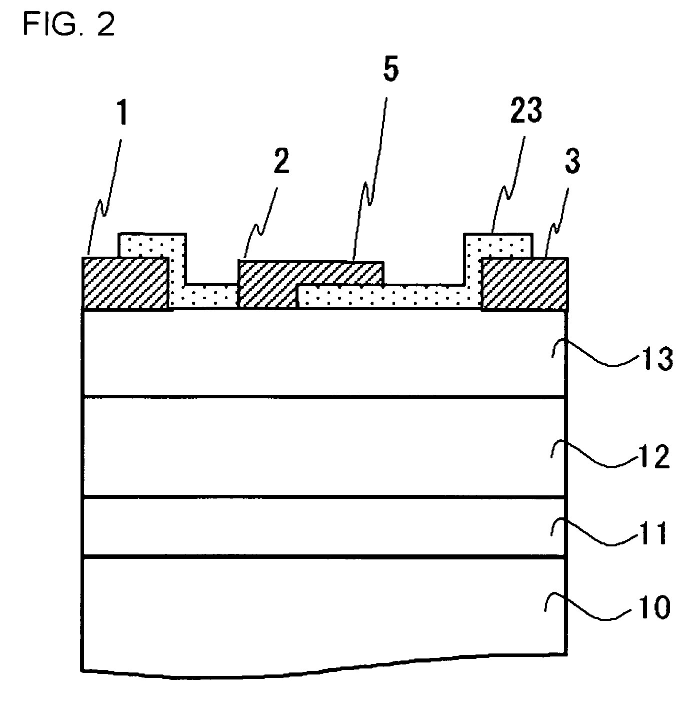
[0105]FIG. 2 shows a sectional structure of HJFET in Example 2. HJFET is formed on the substrate 10 made of the material such as SiC. The buffer layer 11 including the semiconductor layer is formed on the substrate 10. The GaN channel layer 12 is formed on the buffer layer 11. The AlGaN electron supply layer 13 is formed on the GaN channel layer 12. The source electrode 1 and drain electrode 3, in which the ohmic contact is secured, are formed on the electron supply layer. The gate electrode 2, in which the Schottky contact is secured, is provided between the source electrode 1 and the drain electrode 3. The gate electrode 2 has the field plate portion 5 overhanging the drain side in the visored shape. The surface of the electron supply layer 13 is covered with a SiON film 23, and the SiON film 23 is provided immediately below the field plate portion 5.

[0106]HJFET according to Example 2 is formed as follows: At first, the semiconductor is grown on the substrate 10 made of SiC, e.g.,...

example 3

[0111]Referring to FIG. 3, Example 3 of the invention will be described below.

[0112]FIG. 3 shows a sectional structure of HJFET in Example 3. HJFET is formed on the substrate 10 made of the material such as SiC. The buffer layer 11 including the semiconductor layer is formed on the substrate 10. The GaN channel layer 12 is formed on the buffer layer 11. The AlGaN electron supply layer 13 is formed on the GaN channel layer 12. The source electrode 1 and drain electrode 3, in which the ohmic contact is secured, are formed on the electron supply layer. The gate electrode 2, in which the Schottky contact is secured, is provided between the source electrode 1 and the drain electrode 3. The gate electrode 2 has the field plate portion 5 overhanging the drain side in the visored shape. The surface of the electron supply layer 13 is covered with a SiOC film 24, and the SiOC film 24 is provided immediately below the field plate portion 5.

[0113]HJFET according to Example 3 is formed as follow...


PUM


Abstract

A field plate portion (5) overhanging a drain side in a visored shape is formed in a gate electrode (2). A multilayered film including a SiN film (21) and a SiO2 film (22) is formed beneath the field plate portion (5). The SiN film (21) is formed so that a surface of an AlGaN electron supply layer (13) is covered therewith.

Description

[0001]This application is a National Stage application of PCT / JP2003 / 016034, filed Dec. 15, 2003, which claims priority from Japanese patent application JP 2002-364405, filed Dec. 16, 2002. The entire contents of each of the aforementioned applications are incorporated herein by reference.FIELD OF THE INVENTION[0002]The present invention relates to a field-effect transistor in which a Group III nitride semiconductor is used.DESCRIPTION OF THE RELATED ART[0003]Group III nitride semiconductors including GaN have a large band gap, a high dielectric breakdown electric field, and high electron saturation drift velocity. Further, because two-dimensional carrier gas can be utilized by a heterojunction, the Group III nitride semiconductors are expected as a material for realizing an electronic element which is excellent for high-temperature operation, high-speed switching operation, large-power operation, and the like.[0004]In the transistor in which the Group III nitride semiconductor is u...

Claims


Application Information

Patent Timeline
Patent Type & Authority Patents(United States)
IPC IPC(8): H01L31/072H01L21/338H01L29/06H01L29/20H01L29/40H01L29/423H01L29/778H01L29/812
CPCH01L29/402H01L29/42316H01L29/7787H01L29/2003
Inventor OKAMOTO, YASUHIROMIYAMOTO, HIRONOBUANDO, YUJINAKAYAMA, TATSUOINOUE, TAKASHIKUZUHARA, MASAAKI
Owner NEC CORP
Why Eureka
Try Eureka