Structures incorporating semiconductor device structures with reduced junction capacitance and drain induced barrier lowering

a semiconductor device and junction capacitance reduction technology, applied in semiconductor devices, instruments, computing, etc., can solve the problems of slow device performance, inability to adequately balance competing performance drawbacks, and conventional approaches to scaling the channel length of soi mosfets into the deep-submicron rang

Inactive Publication Date: 2011-07-19
GLOBALFOUNDRIES INC
View PDF16 Cites 32 Cited by
  • Summary
  • Abstract
  • Description
  • Claims
  • Application Information

AI Technical Summary

Problems solved by technology

Scaling SOI MOSFETs presents design challenges to the semiconductor industry.
However, thinning the buried insulator layer increases junction capacitance, which slows device performance.
Conventional approaches for scaling the channel length in SOI MOSFETs into the deep-submicron range have been unable to adequately balance the competing performance drawbacks of DIBL and junction capacitance.

Method used


Image

  • Structures incorporating semiconductor device structures with reduced junction capacitance and drain induced barrier lowering
  • Structures incorporating semiconductor device structures with reduced junction capacitance and drain induced barrier lowering
  • Structures incorporating semiconductor device structures with reduced junction capacitance and drain induced barrier lowering

Examples


Embodiment Construction

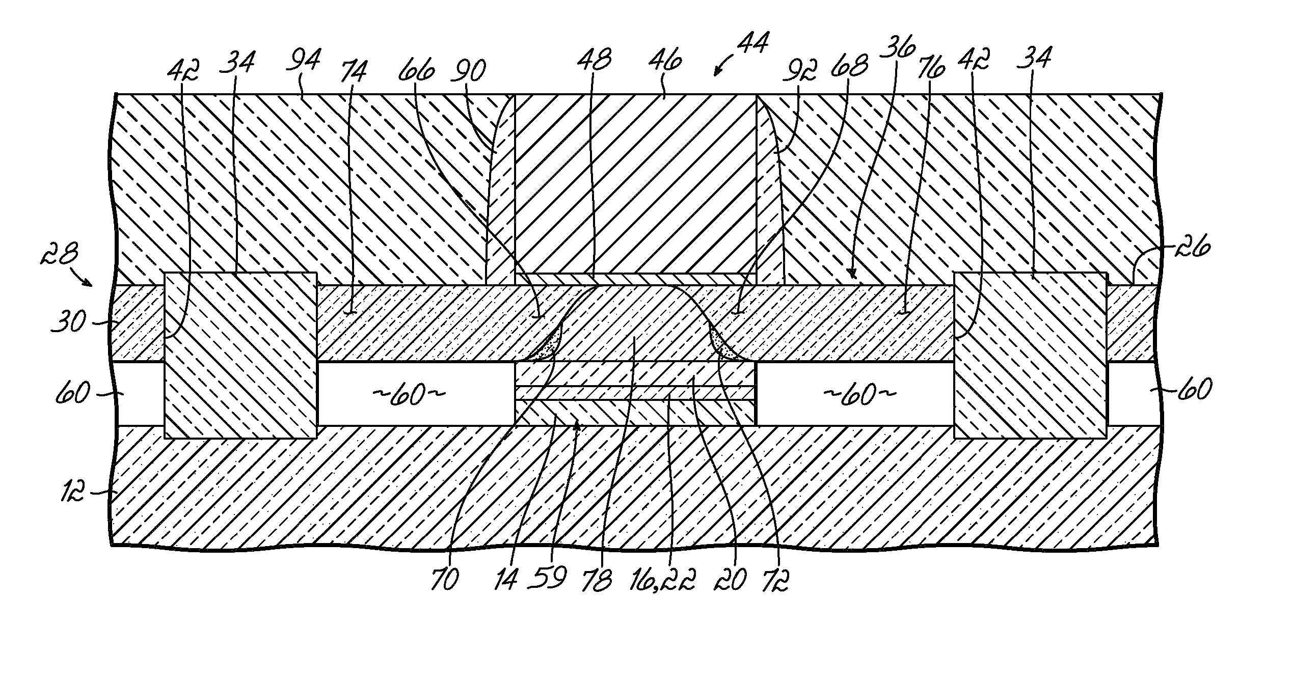
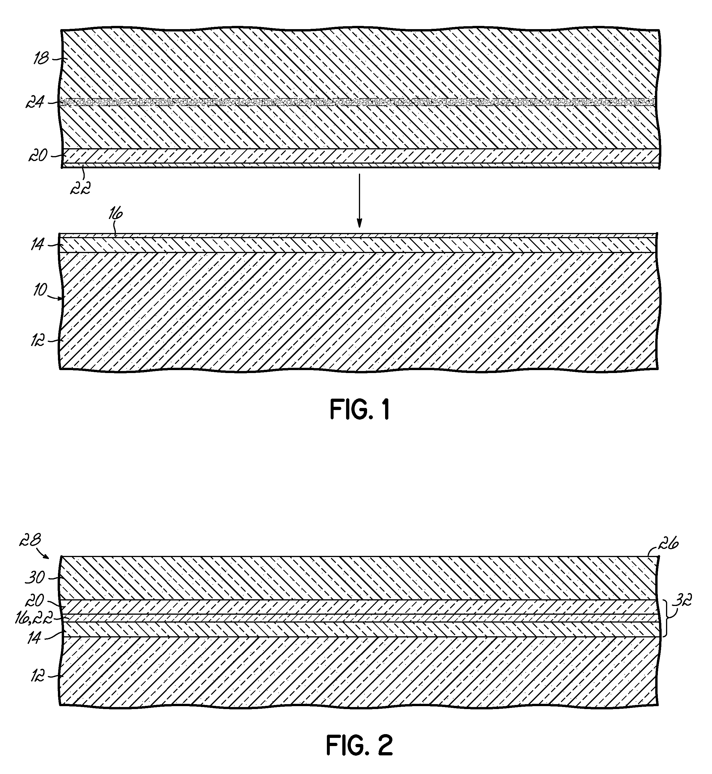
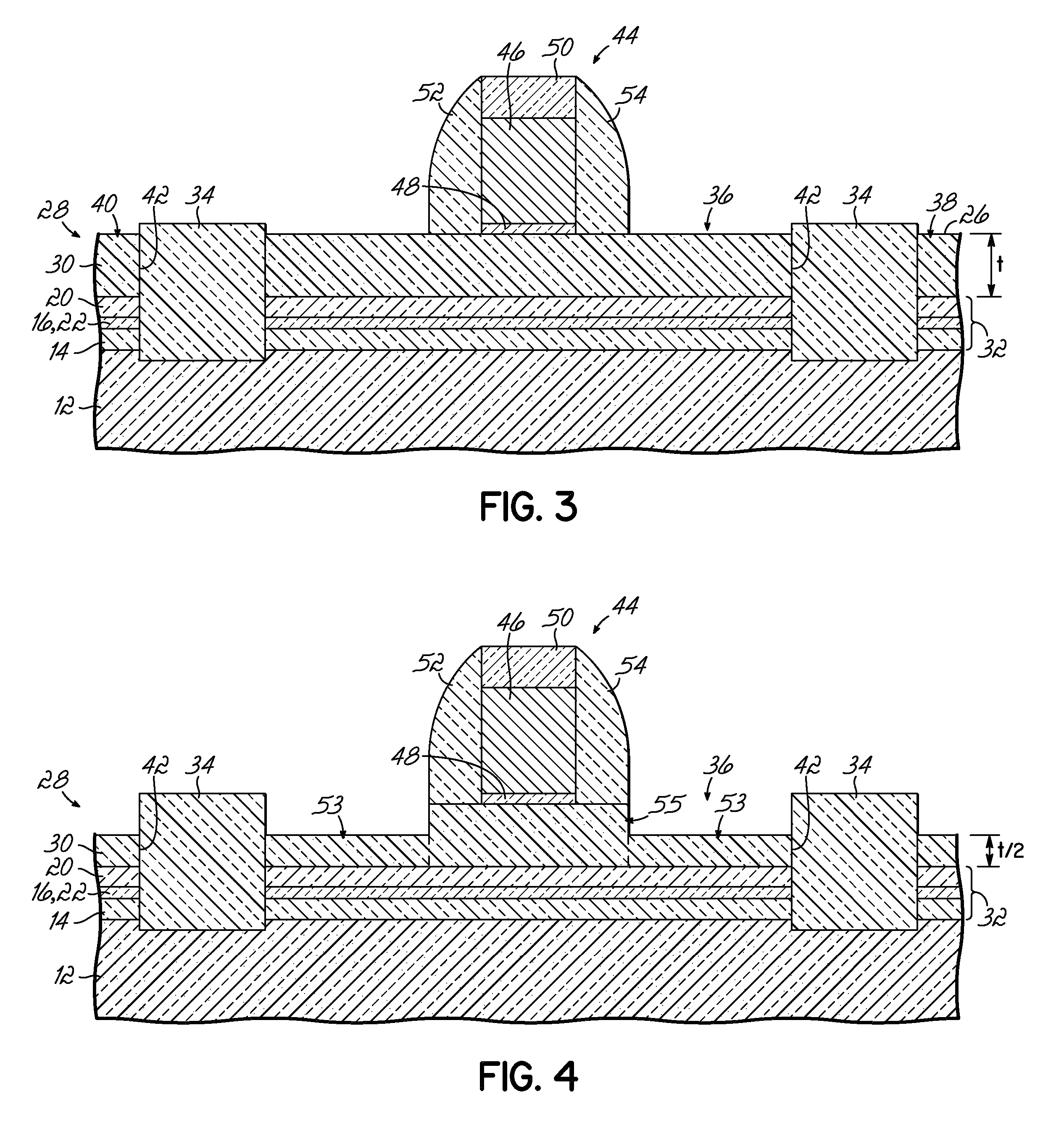
[0020]The invention is directed to semiconductor device structures and fabrication methods for metal-oxide-semiconductor field-effect transistors (MOSFETs) fabricated using semiconductor-on-insulator (SOI) substrates having a composite insulator layer composed of dielectric materials with different dielectric constants that cooperate, when strategically positioned, to balance junction capacitance and drain induced barrier lowering (DIBL) in the MOSFET. Specifically, the semiconductor device structure includes an electrically thin back insulator beneath the channel region of the SOI MOSFET that operates to suppress DIBL and an electrically thick back insulator under the source / drain regions of the SOI MOSFET that acts to reduce the junction capacitance. The region of the back insulator beneath the channel region is formed from a dielectric material having a significantly higher dielectric constant than the dielectric material forming the region of the back insulator beneath the sourc...


PUM


Abstract

Design structure embodied in a machine readable medium for designing, manufacturing, or testing a design. The design structure includes semiconductor device structures characterized by reduced junction capacitance and drain induced barrier lowering. The semiconductor device structure of the design structure includes a semiconductor layer and a dielectric layer disposed between the semiconductor layer and the substrate. The dielectric layer includes a first dielectric region with a first dielectric constant and a second dielectric region with a second dielectric constant that is greater than the first dielectric constant.

Description

CROSS-REFERENCE TO RELATED APPLICATIONS[0001]This application is a continuation-in-part of application Ser. No. 11 / 379,655, filed Apr. 21, 2006, which is hereby incorporated by reference herein in its entirety.FIELD OF THE INVENTION[0002]The invention relates generally to integrated circuit fabrication and, in particular, to design structures including semiconductor device structures with reduced junction capacitance and drain induced barrier lowering.BACKGROUND OF THE INVENTION[0003]Metal-oxide-semiconductor field-effect transistors (MOSFETs) are common semiconductor device structures widely used in the semiconductor industry for switching, amplification, filtering, and other applications related to both analog and digital electrical signals. Conventional planar MOSFETs include a gate electrode overlying a channel region near an upper surface of a semiconductor substrate and a gate dielectric physically separating the gate electrode from the semiconductor material of the channel re...

Claims


Application Information

Patent Timeline
Patent Type & Authority Patents(United States)
IPC IPC(8): G06F17/50H01L29/76
CPCH01L29/66545H01L29/66636H01L29/66772H01L29/78603H01L29/51H01L29/513G11C29/54
Inventor CHENG, KANGGUOHSU, LOUIS LU-CHENMANDELMAN, JACK ALLANYANG, HAINING
Owner GLOBALFOUNDRIES INC
Why Eureka
Try Eureka