Method for manufacturing SOI substrate using cluster ion

a technology of cluster ion and soi substrate, which is applied in the direction of semiconductor/solid-state device manufacturing, basic electric elements, electric apparatus, etc., can solve the problems of reducing the thickness deteriorating the takt time, and affecting the efficiency of the soi substrate, so as to achieve the effect of reducing the thickness, reducing the cost, and reducing the cos

Inactive Publication Date: 2011-08-02
SEMICON ENERGY LAB CO LTD
View PDF57 Cites 11 Cited by
  • Summary
  • Abstract
  • Description
  • Claims
  • Application Information

AI Technical Summary

Benefits of technology

[0011]In view of the foregoing problems, the present invention provides a manufacturing method of an SO substrate, by which resources can be effectively used. The present invention provides a method for manufacturing SOI substrates with high throughput. The present invention provides a manufacturing method of an SOI substrate, which leads to cost reduction. The present invention provides a method for manufacturing SOI substrates with high yield.
[0023]By irradiating a semiconductor wafer with cluster ions, a separation layer for separating a semiconductor layer can be formed efficiently at a small depth from the surface of the semiconductor wafer. Consequently, the semiconductor layer to be separated can be made thin, so that a larger thickness of a separation wafer which is to be reused is attainable and takt time can be shortened. Accordingly, SOI substrates can be manufactured with effective use of resources and high throughput. Further, cost reduction can be achieved.
[0024]By employing the manufacturing method of an SOI substrate, in which repetitive reusing of a separation wafer is presupposed, SOI substrates can be manufactured with high yield even when a separation wafer is repeatedly used.

Problems solved by technology

A semiconductor wafer, which is a material of an SOI substrate, is expensive; thus, reusing of the separation wafer leads to cost reduction.
However, in an ion implantation method used in a conventional hydrogen ion implantation separation method, hydrogen ions for irradiation of a semiconductor wafer are small in mass, so that hydrogen tends to be implanted at a large depth from the surface of the semiconductor wafer.
An attempt to increase the thickness of the separation wafer obtained through separation by implanting hydrogen at a small depth of a semiconductor wafer requires reduction in an accelerating voltage, which leads to deterioration of takt time and degradation of throughput.
Further, when reusing of the separation wafer is repeated, the quality as a semiconductor wafer inevitably deteriorates, which provides a possibility to result in quality deterioration of an SOI substrate manufactured using the semiconductor wafer.
In addition, repeated reuse of the separation wafer causes a problem such as generation of a crack in the semiconductor wafer in the process for manufacturing an SOI substrate, decreasing the yield of SOI substrates.

Method used


Image

  • Method for manufacturing SOI substrate using cluster ion
  • Method for manufacturing SOI substrate using cluster ion
  • Method for manufacturing SOI substrate using cluster ion

Examples


embodiment mode 1

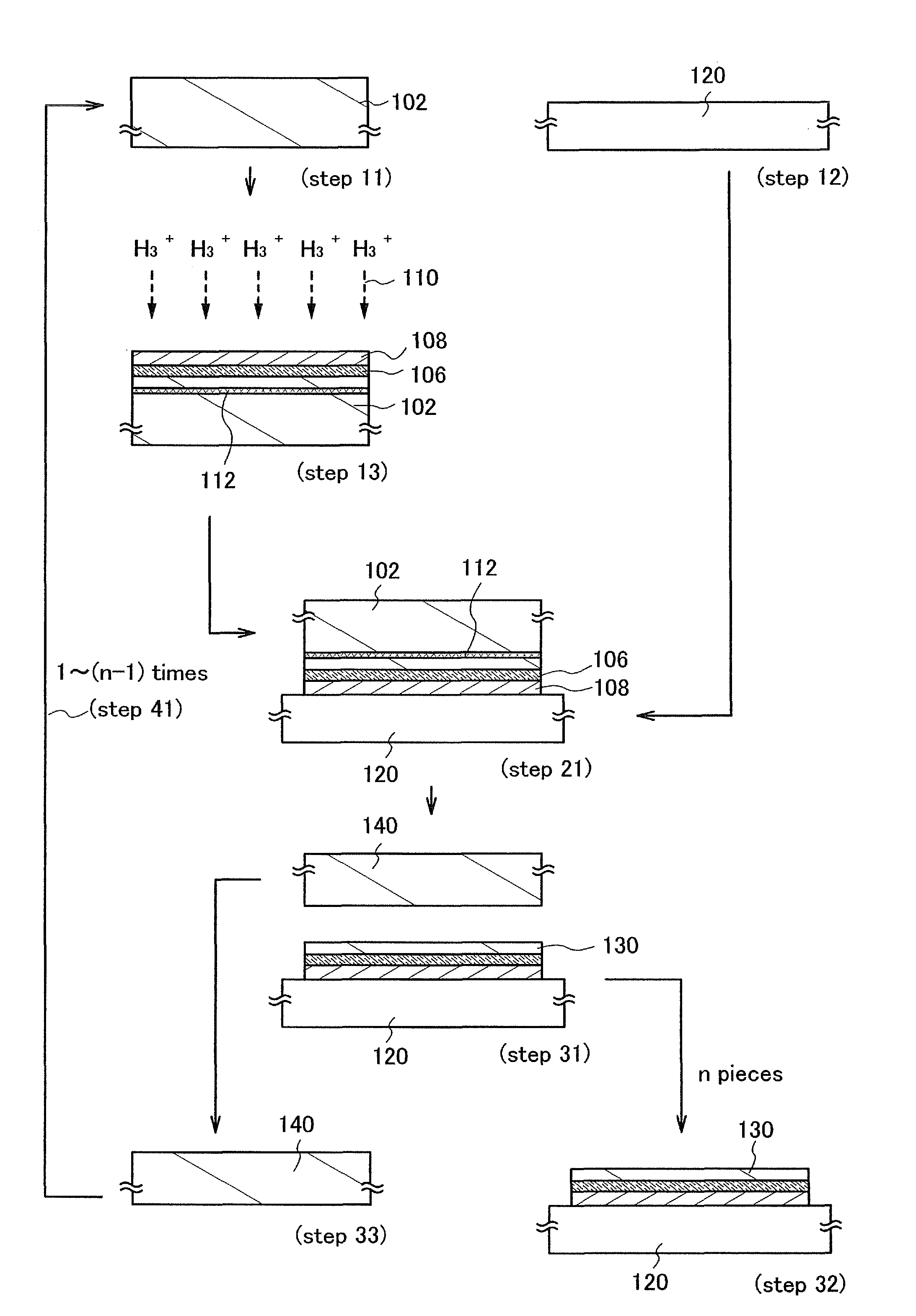
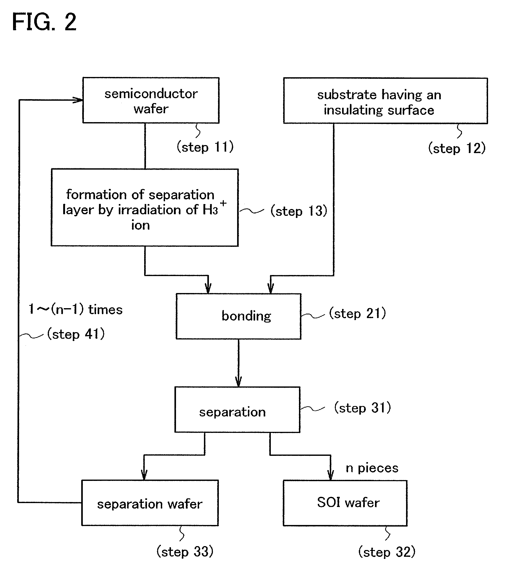
[0049]In a manufacturing method of an SOI substrate of this embodiment mode, a semiconductor layer separated from a semiconductor wafer which is a bond substrate is bonded to a base substrate to manufacture an SOI substrate. After the semiconductor layer is separated, a separation wafer is subjected to treatment for reusing and reused as a bond substrate. An example of an SOI substrate and its manufacturing method of this embodiment mode will be described below with reference to drawings.

[0050]A bond substrate and a base substrate are prepared. A semiconductor wafer 102 and a substrate having an insulating surface 120 are prepared as the bond substrate and the base substrate, respectively (see (step 11) and (step 12) in FIGS. 1 and 2).

[0051]As the semiconductor wafer 102, a semiconductor wafer of silicon, germanium, or the like, or a compound semiconductor wafer of gallium arsenide, indium phosphide, or the like is used, for example. Preferably, a single crystal semiconductor wafer ...

embodiment mode 2

[0103]The example of (1) in which the first insulating layer 106 is formed, the semiconductor wafer 102 is irradiated with the cluster ions 110 from the surface side where the first insulating layer 106 is formed to form the separation layer 112, and then, the second insulating layer 108 is formed over the first insulating layer 106 in (step 13) is described in Embodiment Mode 1. In Embodiment Mode 2, the following examples will be described: the example of (2) in which the first insulating layer 106 is formed, the second insulating layer 108 is formed over the first insulating layer 106, and then, the semiconductor wafer 102 is irradiated with the cluster ions 110 from the surface side where the first insulating layer 106 and the second insulating layer 108 are stacked so that the separation layer 112 is formed; and the example of (3) in which a protective layer 103 is formed over one surface of the semiconductor wafer 102, the protective layer 103 is irradiated with the cluster io...

embodiment mode 3

[0115]In this embodiment mode, the hydrogen concentration distribution when hydrogen is implanted into the semiconductor wafer in Embodiment Mode 1 or 2 will be described.

[0116]With the ion doping apparatus, irradiation of a semiconductor wafer (a silicon wafer with a crystal orientation of a (100) plane) with H3+ or H+ ions was performed. Then, based on the resulting data on secondary ion mass spectrometry (SIMS) analysis, a model of hydrogen implantation was established and the concentration of hydrogen in a depth direction was calculated. The calculation was performed in the following condition: the size of the model is (x-axis, y-axis, z-axis)=(800 nm, 800 nm, 1200 nm). Note that the x-axis and y-axis corresponds to a plane surface of the semiconductor wafer and the z-axis corresponds to a depth direction. Further, in the ion doping apparatus used in the experiment, the wafer was rotated in order to uniform the hydrogen implantation distribution.

[0117]The number of hydrogen atom...


PUM


Abstract

A method is demonstrated to manufacture SOI substrates with high throughput while resources can be effectively used. The present invention is characterized by the feature in which the following process A and process B are repeated. The process A includes irradiation of a surface of a semiconductor wafer with cluster ions to form a separation layer in the semiconductor wafer. The semiconductor wafer and a substrate having an insulating surface are then overlapped with each other and bonded, which is followed by thermal treatment to separate the semiconductor wafer at or around the separation layer. A separation wafer and an SOI substrate which has a crystalline semiconductor layer over the substrate having the insulating surface are simultaneously obtained by the process A. The process B includes treatment of the separation wafer for reusing, which allows the separation wafer to be successively subjected to the process A.

Description

BACKGROUND OF THE INVENTION[0001]1. Field of the Invention[0002]The present invention relates to an SOI (silicon on insulator) substrate and a manufacturing method thereof. Further, the present invention relates to a semiconductor device manufactured using the SOI substrate.[0003]Note that a semiconductor device in this specification refers to any device which can function by utilizing semiconductor characteristics, and includes electro-optic devices (including EL display devices and liquid-crystal display devices), semiconductor circuits, and electronic devices in its category.[0004]2. Description of the Related Art[0005]With development of VLSI technology, lower power consumption and higher operation speed transcending the scaling law which governs the performance of semiconductor devices using bulk single crystal silicon have been demanded. In order to satisfy these requirements, an SOI structure has received attention in recent years. This technology allows an active region (cha...

Claims


Application Information

Patent Timeline
Patent Type & Authority Patents(United States)
IPC IPC(8): H01L21/76H01L21/30H01L21/46
CPCH01L21/76254H01L21/302
Inventor OHNUMA, HIDETOYAMAZAKI, SHUNPEI
Owner SEMICON ENERGY LAB CO LTD
Why Eureka
Try Eureka