
Methods and apparatus for reallocating addressable spaces within memory devices

a memory device and addressable space technology, applied in the field of integrated circuit systems, can solve problems such as device failure, generating threshold voltage, and reducing the effective lifetime of an eeprom devi

Active Publication Date: 2011-08-16
SAMSUNG ELECTRONICS CO LTD
View PDF7 Cites 8 Cited by
  • Summary
  • Abstract
  • Description
  • Claims
  • Application Information

AI Technical Summary

Benefits of technology

The present invention relates to integrated circuit systems with non-volatile memory devices and memory processing circuits. The memory processing circuit is configured to adjust the capacity of the non-volatile memory device by increasing the number of physical addresses that map to the device. This is done by using an address transformation table to generate physical addresses that map to the non-volatile memory device. The memory processing circuit can also read the memory allocation region to determine the capacity of the active and reserved memory regions and write data into the region to modify the allocation. The technical effect of this invention is to provide a more efficient and flexible way to adjust the capacity of non-volatile memory devices.

Problems solved by technology

Unfortunately, performing a relatively large number of erase operations on a block of EEPROM cells may result in the generation of “threshold-voltage” defects within one or more EEPROM cells and thereby reduce an effective lifetime of an EEPROM device.
However, once all available reserved memory blocks have been utilized to replace respective active memory blocks, then the detection of any further defects within the EEPROM device during subsequent erase and programming operations may result in device failure.
Nonetheless, because many of the active memory blocks may have different susceptibilities to defects caused by erase / program operations, the techniques to relatively evenly distribute erase / program operations across multiple active memory blocks may not be entirely successful in achieving relatively long device lifetimes.

Method used


Image

  • Methods and apparatus for reallocating addressable spaces within memory devices
  • Methods and apparatus for reallocating addressable spaces within memory devices
  • Methods and apparatus for reallocating addressable spaces within memory devices

Examples


Embodiment Construction

[0012]The present invention will now be described more fully hereinafter with reference to the accompanying drawings, in which preferred embodiments of the invention are shown. This invention may, however, be embodied in different forms and should not be construed as limited to the embodiments set forth herein. Rather, these embodiments are provided so that this disclosure will be thorough and complete, and will fully convey the scope of the invention to those skilled in the art. Like numbers refer to like elements throughout.

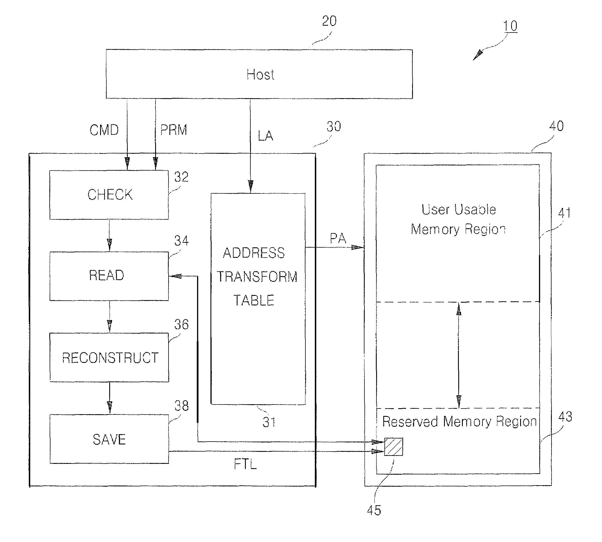
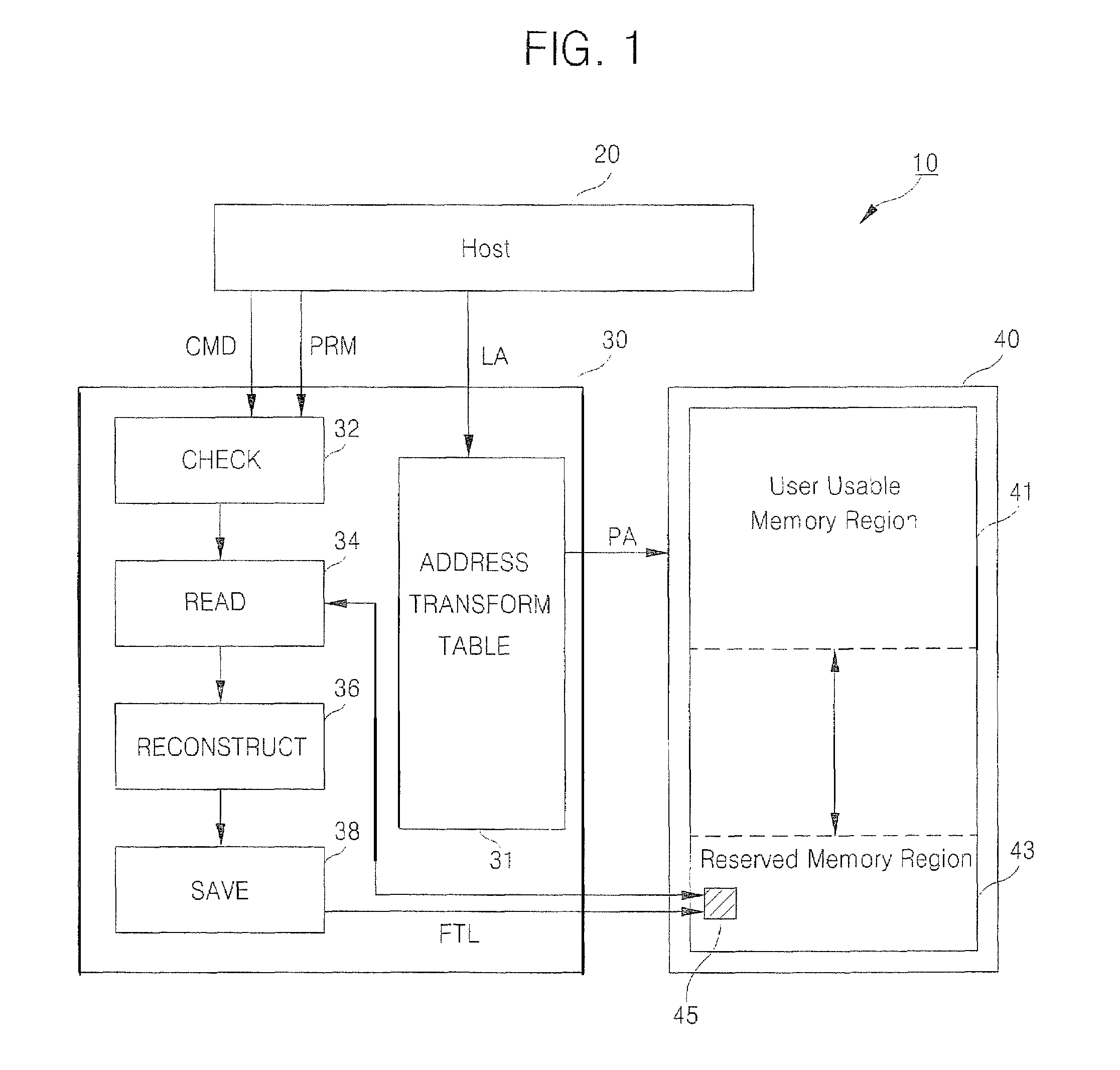
[0013]FIG. 1 illustrates an integrated circuit system 10 according to an embodiment of the present invention. This system 10 is illustrated as including a host processor 20, a memory processor 30 and a non-volatile memory device 40, connected as illustrated. The memory processor 30 and the non-volatile memory device 40 may be treated herein as a memory capacity adjusting device. This system 10 may be embodied within a video camera, television, audio system, gam...


PUM


Abstract

Integrated circuit systems include a non-volatile memory device (e.g, flash EEPROM device) and a memory processing circuit. The memory processing circuit is electrically coupled to the non-volatile memory device. The memory processing circuit is configured to reallocate addressable space within the non-volatile memory device. This reallocation is performed by increasing a number of physical addresses within the non-volatile memory device that are reserved as redundant memory addresses, in response to a capacity adjust command received by the memory processing circuit.

Description

CROSS-REFERENCE TO RELATED APPLICATION[0001]This application claims priority to Korean Patent Application No. 10-2006-0101644, filed Oct. 19, 2006, the disclosure of which is hereby incorporated herein by reference.FIELD OF THE INVENTION[0002]The present invention relates to integrated circuit systems and, more particularly, to processors for controlling memory devices and methods of operating memory devices.BACKGROUND OF THE INVENTION[0003]Non-volatile memory devices, such as flash EEPROM devices, have many advantageous characteristics that make them suitable for use in low-power applications. These low-power applications include mobile device applications, such as digital cameras, MP3 music players, cellular telephones, memory cards and personal digital assistants (PDA).[0004]As will be understood by those skilled in the art, operations to program flash EEPROM devices are typically automatically preceded by erase operations (e.g., block erasure), which prepare EEPROM cells within ...

Claims


Application Information

Patent Timeline
Patent Type & Authority Patents(United States)
IPC IPC(8): G06F12/00
CPCG06F12/0246G06F2212/7211G06F2212/1036G06F9/06G06F12/00
Inventor IM, JUNG-BEENKIM, HYE-YOUNGCHOI, YOUNG-JOONLEE, DONG-GILEE, SHEA-YUN
Owner SAMSUNG ELECTRONICS CO LTD
Learn More