Storage system disposed with plural integrated circuits

a storage system and integrated circuit technology, applied in the field of storage systems disposed with plural integrated circuits, can solve the problems of poor buffer utilization efficiency, large logic gate scale (mounting area) and small number of the pci-express interface circuit component that is installed on the adapter, so as to improve the buffer utilization efficiency

Inactive Publication Date: 2011-08-30
HITACHI LTD
View PDF14 Cites 165 Cited by
  • Summary
  • Abstract
  • Description
  • Claims
  • Application Information

AI Technical Summary

Benefits of technology

Consequently, it is an object of the present invention to provide a transceiving technology that controls the mounting area of a circuit pertaining to transmission and / or reception and where the utilization efficiency of a buffer is improved.
Further, it is another object of the present invention to achieve the above-described object without changing the algorithms of layers (e.g., the aforementioned PL, DLL and TL) inside the interface component.

Problems solved by technology

As shown in FIG. 1 and FIG. 2, when plural buffers that respectively correspond to the plural TLP types are prepared, there are instances where the utilization efficiency of the buffers becomes bad.
However, when the capacity of each of the buffers is made into the above-described capacity, the logic gate scale (mounting area) of the PCI-Express interface circuit component ends up becoming large.
This is a problem particularly in a storage system.
The reason is because, in a storage system, it is desired that the paths between the LSIs (PCI-Express lanes) be made redundant, and for this reason, plural PCI-Express interface circuit components become necessary for each of the adapters and the switch circuit, but as described above, when the mounting area of the PCI-Express interface circuit components ends up becoming large, the number of the PCI-Express interface circuit components that are installable on the adapters and the switch circuit ends up becoming small, and therefore making the paths between the LSIs redundant can become difficult.
However, when the buffers are made into a large capacity, both the problem that the logic gate scale of the PCI-Express interface circuit components ends up becoming large and the problem that utilization efficiency is bad, where useless areas that are not utilized are present in the buffers even when a certain type of TLP flows at the limit performance of PCI-Express, arise.
The above problems are problems that can exist even in transmission and reception utilizing an interface other than PCI-Express.

Method used


Image

  • Storage system disposed with plural integrated circuits
  • Storage system disposed with plural integrated circuits
  • Storage system disposed with plural integrated circuits

Examples


Embodiment Construction

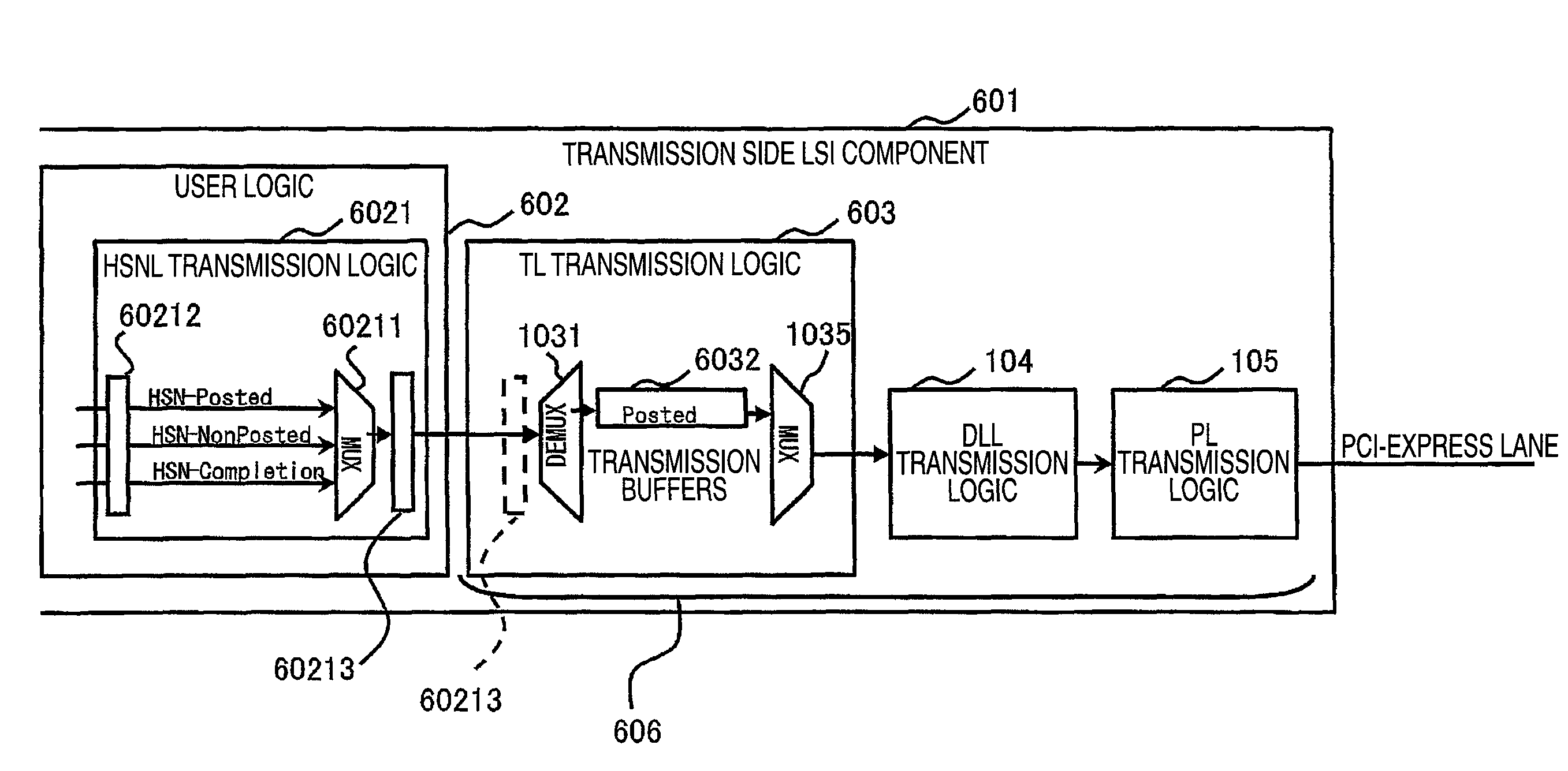
Below, an embodiment of the present invention will be described with reference to the drawings.

FIG. 5A shows the configuration of a storage system pertaining to the embodiment of the present invention.

The storage system is a disk array device such as a RAID (Redundant Array of Independent Disks), for example. The storage system is, for example, disposed with a disk controller (below, DKC) 501 that controls processing that the storage system performs and a disk unit (below, DKU) 502 that includes plural hard disk drives (HDDs) 5021. Instead of the HDDs 5021, another type of storage device (e.g., a flash memory device) may also be disposed.

The DKC 501 is disposed with LRs (Local Routers) 5011 and 5012, an SW (Switch) 5013, a CMA (Cache Memory Adapter) 5014, a CM (Cache Memory) 5015, an MPA (Micro Processor Adapter) 5016, an MCH (Memory Controller Hub) 5017, an MP (Micro Processor) 5018 and an LM (Local Memory) 5019.

“LR” is an abbreviation for local routers, and the local routers are L...


PUM


Abstract

To provide a transceiving technology that controls the mounting area of a circuit pertaining to transmission and / or reception and where the utilization efficiency of a buffer is improved. In a transmission side circuit, there are disposed a transmission side first circuit component that generates a first packet that follows a request and a transmission side second circuit component that is a lower-level circuit component of the transmission side first circuit component, includes a transmission buffer and temporarily stores in the transmission buffer, and transmits, a second packet that includes the first packet. The second packet includes a second header portion and a second data portion. In the second data portion that the second packet that is transmitted from the transmission side second circuit component includes, there is included the first packet, and in the second header portion, there is included a predetermined value as a parameter value that represents the type of the second packet. The predetermined value is a value that represents a predetermined one second packet type of plural second packet types.

Description

CROSS REFERENCES TO RELATED APPLICATIONSThis application relates to and claims priority from Japanese Patent Application No. 2008-215003, filed on Aug. 25, 2008, the entire disclosure of which is incorporated herein by reference.BACKGROUND OF THE INVENTION1. Field of the InventionThe present invention relates to a storage system disposed with plural integrated circuits.2. Description of the Related ArtA storage system is disposed with plural storage devices and a controller that accesses at least one storage device of the plural storage devices in accordance with an access request from a higher-level device. The controller is, for example, disposed with a cache memory that temporarily stores data that are to be written in the storage devices or are to be read from the storage devices, a microprocessor that controls the reading and writing of data with respect to the storage devices, an interface circuit (a higher-level adapter) with the higher-level device (e.g., a host computer or ...

Claims


Application Information

Patent Timeline
Patent Type & Authority Patents(United States)
IPC IPC(8): G06F3/00G06F5/00G06F13/00G06F13/42
CPCG06F13/385H04L49/90H04L49/9063G06F3/0613G06F3/0658G06F3/0689
Inventor IWAOKA, YOMORITOKI, NAOKI
Owner HITACHI LTD
Why Eureka
Try Eureka